Blind via and buried via PCB in PCB Design and Manufacturing
What are Blind and Buried Vias
A topic that often comes up when discussing printed circuit board manufacturing is blind and buried vias. Here we’ll discuss what these are and how they can help you receive PCBs that function the way you intend. We’ll review the benefits of blind and buried vias, how they’re built, and why it’s vital to work with an experienced PCB manufacturer that knows how to properly add blind and buried vias to printed circuit boards.
It can often be difficult to fit all the needed connections on a PCB onto a single layer. A way around this problem is with vias. They are conductive holes that are shaped similar to a barrel, which allows for connections across multiple layers of the PCB. While there are several vias, there are two that are used most often. These are the blind and buried vias, and we believe they can provide some excellent benefits to those who use them in their PCBs.
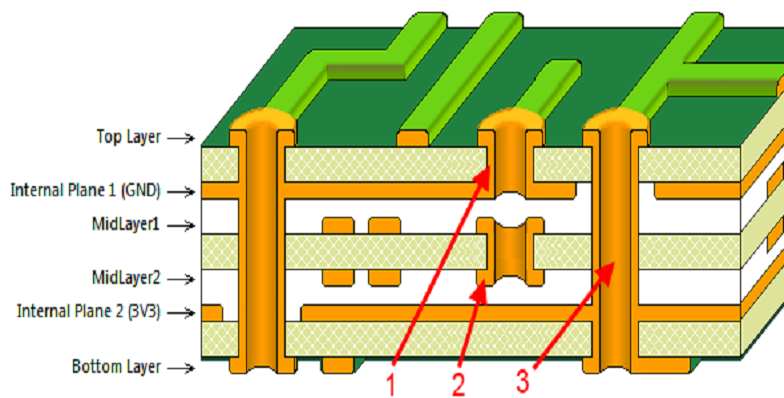
Blind and buried vias are controlled depth vias commonly used in HDI PCB boards. Here interconnection is established without consuming more space on the PCB, thus making more room for the increased wiring density. Since through holes consume more board real-estate, the space available for wiring is reduced. Hence, blind and buried are preferred.
Blind and buried vias provide electrical connections from the outer layers to the inner layers as well as in between the inner layers, and are used when you have limited space on your PCB. Buried vias are hidden beneath the layers and free up surface space without impacting the traces or surface components on the top or bottom layers. Blind vias also free up space, can be essential for fine pitch BGA components and have the added benefit of helping reduce signal stubs through the drilling process as the via terminates at the last connected layer.
You mostly see blind and buried vias in High density interconnect (HDI) PCBs. HDIs provide benefits such as increased layer density, improved power delivery and use of much smaller pitch devices. The hidden vias help keep the board light and compact. It is common to see blind and buried vias in electronic products like, cell phones, laptops, and medical devices to name a few.
Incorporating blind and buried vias make more connections and higher board density possible. But not without drawback. Vias add extra steps to manufacturing and testing, which come with added costs.
What is blind via
A blind via will connect an outer layer of the board to one of the inner layers. However, it does not go all the way through the entire PCB. It is a connection from an outer layer of a board to one or more inner layers without exiting out the opposite side of the board. When a via starts on one side of a PCB but does not pass all the way through, it is called a blind via. Blind vias are common in high density interconnect (HDI) PCBs. The added complexity of blind vias allows designers to improve signal integrity while reducing PCB size. Using blind vias presents a range of new routing alternatives and options as valuable space is no longer needed for through-hole vias, which travel through layers where they are not connected to.
The holes for each connection level must be defined as a separate drill file.
The ratio of drill diameter to hole depth (aspect ratio) must be 1:1 or larger.
The smallest hole determines the depth and thus the max. distance between the
outer layer and the corresponding inner layers.
Blind Vias
When a via starts on one side of a PCB but does not pass all the way through, it is called a blind via. The four types of blind vias are:
- Photo defined blind vias.
- Sequential lamination blind vias
- Controlled depth blind vias.
- Laser drilled blind vias.
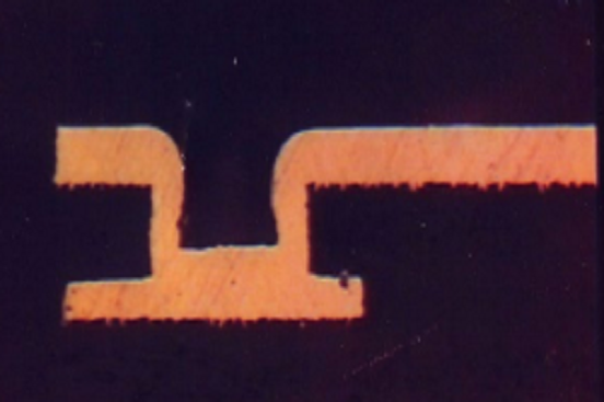
Photo Defined Blind Via: A photo defined via is created by laminating a sheet of photosensitive resin to a core (This core is comprised of laminated layers that may contain the power planes as well as some buried signal layers). The layer of photosensitive material is covered with a pattern that covers the areas where the holes are to be created and is then exposed to light of a wavelength that will cause the remaining material on the PCB to harden. Following this, the PCB is immersed in an etching solution that removes the material in the holes. This creates a path to the next layer down. After the etching process, copper is plated in the hole and on the outer surface to create the outer layer of the PCB. This operation is normally done on both sides of the PCB at once, and adds a layer to each side.
Photo-defined vias are commonly used to create multilayer organic BGA (ball grid array) packages and cell phone PCBs. The advantage in using them is that it costs the same to create thousands of blind vias as it does to create just one. When only a few blind vias are required, their use becomes a cost disadvantage.
Sequential Lamination Blind Via: A sequential laminate blind via is created by processing a very thin piece of laminate through all of the steps involved in creating a two-sided PCB. The laminate is drilled, plated, and etched to define the features in the side that will form layer 2 of the board. The other side is left as a solid sheet of copper, and it will form layer 1 of the finished PCB. The subassembly is then laminated with all of the other layers of the PCB. The resulting combined lamination is then processed through all of the steps involved in creating the outer layers of a multilayer PCB. Sequential lamination blind vias were used in the creation of many of the early cell phone PCBs. It is the most expensive way to form blind vias due to the extra process steps required and the yield loss associated with handling very thin laminates through the drilling, etching and plating operations. As a result, it should be considered the last resort when blind vias are required.
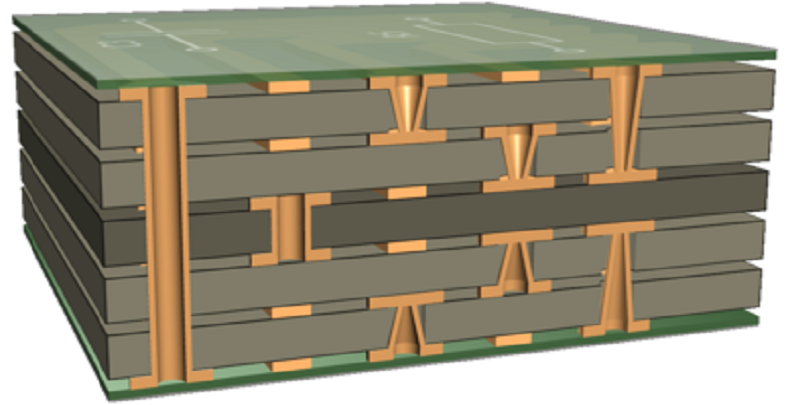
Controlled Depth Drilled Blind Vias: As can be seen from Figure 1, controlled-depth blind vias are created in the same way as through-hole vias. Here, the drill is set to penetrate only partway through the PCB. The designer of the artwork places a pad on layer 2 that is pierced by the drill. Care is taken to ensure there are no features below the drilled hole that may come in contact with the drilled hole. Copper is then plated in the drilled hole at the same time that copper is plated in the through-hole vias.
Controlled-depth vias are the least expensive type of blind via as no additional equipment or process steps are required to create them. The limitations of these vias are the holes must be large enough for mechanical drills to create them and the area below them must be kept clear of circuits that might be accidentally touched by the drilled hole.
Laser Drilled Blind Vias: These are created after all of the layers in a PCB have been laminated and before the outer layer has been etched and plated. A laser is used to ablate the copper on the outer layer as well as the insulating material between layers 1 and 2.
Why are Blind Vias used?
Vias in signal lines are plagued with the parasitic capacitance that is created by the barrel of the plated through-hole and the planes through which it passes. This parasitic capacitance is primarily a function of the area of the outside of the plated through-hole which is a cylinder passing through the PCB. This area is determined by the diameter of the drill and the PCB thickness. With today’s high data rates, this parasitic capacitance can degrade the signal beyond where it can be successfully used. Therefore, there has to be some method for reducing this parasitic capacitance. Blind vias do this by shortening the length of the vias and reducing their diameters. As a result, blind vias are a good way to connect signal lines that operate above 4.8 Gb/s.
Blind Via PCB
Blind vias connect an outer layer of a PCB to one or more inner layers without penetrating the entire board. As the name suggests, these vias are “blind” because they are not visible from the opposite side of the PCB. Blind vias offer several advantages, such as saving space on the board, enabling more compact designs, and improving signal integrity by reducing the length of signal paths.
Blind vias are drilled through the PCB’s surface layer and only extend a portion of the way through the board, linking the surface layer to one or more inner layers. They are a crucial component in current PCB design, allowing surface-layer components to be connected to inside layers while minimizing the number of layers necessary for routing.
Blind via pcb manufacturing considerations
Blind through hole production challenges include the necessity for accurate drilling and plating operations, which might raise manufacturing costs. Although laser drilling technology can enhance precision and save costs, it may only be appropriate for some PCB designs.
The aspect ratio of the vias, which is the ratio of the diameter to the depth of the via, must also be considered by designers. Larger aspect ratios might be more challenging, increasing costs and possible manufacturing problems.
Applications of blind vias include high-density interconnect (HDI) boards, where space is at a premium, and high-speed digital circuits, where signal integrity is crucial. Blind vias are typically more expensive to manufacture than through-hole vias, but their benefits often outweigh the added cost in demanding applications.
What is buried via
A buried via is located within the board and will connect the inner layers without reaching the outer layers. Buried vias are also called hidden vias since they are not visible when observed from the external layers. These vias are meant for connecting the inner layers of the circuit board. Therefore, space will be available on other layers for wiring.
Blind vias are plated through hole connections that pass from an outside layer and end on an internal layer. They do not pass all the way through the PCB like a conventional via hole. Blind vias aren’t cost effective, unless used for a technical reason such as permitting the fan out of tracking from a fine pitch foot-print. The use of blind vias just to reduce the PCB layer count will not save costs.
The IPC standards suggest that the diameter of the blind and buried vias should be 6 mils (150μm) or less.
Buried Via PCB
Buried vias are plated connections between the inner layers of a multi-layer PCB that do not emerge on either of the outer layers. Buried vias are created by drilling and copper plating the inner layer core (pairs) of a multi-layer PCB in the same way as a standard 2 layer or indeed for a multi-layer plated through hole PCB.
Unlike blind vias, buried vias connect two or more inner layers of a PCB without any connection to the outer layers. They are entirely hidden within the board and cannot be seen from either side. This feature allows designers to use the outer layers of the board for other purposes, such as placing components or routing traces, without interference from Vias.
The primary advantage of buried vias is the increased density they enable in PCB designs. This is particularly useful in multilayer PCBs, where space for routing traces and placing components is limited. However, the production of buried vias is more complex and costly than through-hole vias, requiring additional manufacturing steps such as sequential lamination and drilling.
Advantages of using Buried Via PCB
- Increased density: Buried vias, which connect the inner layers of the PCB without extending to the top layers, can help enhance the density of components on the board.
- Reduced layer count: Buried vias can assist in reducing the number of routing layers necessary, resulting in lower manufacturing costs.
- Improved signal performance: Signal routing through buried vias can reduce crosstalk and EMI between traces, improving signal quality and reliability.
What is the Difference Between Blind and Buried Vias?
A blind via will connect an outer layer of the board to one of the inner layers. However, it does not go all the way through the entire PCB. A buried via is located within the board and will connect the inner layers without reaching the outer layers. There is also a through-hole, which goes through the entire board vertically and will connect all the layers. It is a relatively simple concept to understand, and it can provide some excellent benefits.
How Are the Blind and Buried Vias Built?
The vias can be made either before or after the multilayer lamination. The blind and buried vias are added to the PCB through drilling, which can be precarious. It is important that the builder understands and is aware of the depth of the drill. If the hole is not deep enough, it might not provide a good connection. On the other hand, if the hole is too deep, there is a chance that it could degrade the signal or cause distortion. If any of these things were to occur, it would not be viable.
In a blind via, the hole will need to be defined using a separate drill file. The ratio of that hole diameter to the drill diameter needs to be equal to one or less. With a smaller hole, the distance between the outer layers and the inner layers will be smaller.
With a buried via, each of the holes needs to be made using a separate drill file. This is because they connect to different parts of the inner layer of the boards. The hole depth to drill diameter ratio will need to be no larger than 12. If it is larger than that, it will run the risk of touching other connections within the board.
We recommend working with Hemeixin for PCB manufacturing. This will help to ensure that the design and the build of the board, including the blind and buried vias, are feasible. Failure to prepare and to work with a quality board manufacturer could end up in added costs.
Our experts have the tools and techniques to ensure proper drill depths. We can ensure that there is no air trapped in the PCB during the process. The plating will be applied properly to connect the internal layers.
How Do PCB manufacturer Make Blind and Buried Vias?
Vias are manufactured in two ways: either after or before multilayer lamination. When blind and buried vias are created, one or more of the cores are drilled and the through holes are plated. Then the stack is built and pressed. You can read more about the manufacturing process in the IPC-2221B manual.
When creating blind vias, it is important to be aware of the drill depth. Depending on how shallow or deep the hole is, it could have a negative impact on the board. If the hole is too deep then it may cause signal distortion or degradation, and if it’s too shallow then it could result in an improper connection.
For drilling blind and buried vias, controlled-depth drilling methods are chosen.
The drilling process of controlled depth blind vias is quite similar to that of the through-holes. The only difference is that the drilling source is programmed to stop after one or two layers. Care should be taken to ensure that the drilled hole does not have any connection with the layers underneath it. Then the hole is copper plated and made conductive.
Before drilling buried vias, the inner layers are drilled first. Next, the other layers are pressed to complete the stack-up.
It’s best to consult with your PCB manufacturer to get advice on the best approach to design your board to avoid a costly manufacture. Make sure to have your manufacturer plug the vias with either metal or thermal/electrical epoxy and plate copper over it; or else internal air bubbles can migrate upwards and lead to voids or pin holes in the solder joint.
Sometimes, you can’t fit all your connections on one layer. This is where vias come to your rescue!
Vias are barrel shaped vertical conductive holes that make connections between multiple layers of a PCB. The IPC defines eight different types of vias, but we’re going to talk about blind and buried vias; the two you’re most likely to work with.
A blind via connects an outer layer of the board to inner layers and doesn’t go through the entire board. A buried via connects inner layers without reaching the outer layers. And a through hole via goes all the way through, from top to bottom, connecting all layers.


