HDI Flex PCB
For more than a decade, Hemeixin has continuously innovated next-generation µVia technologies. As the conventional laser via plating technology reached its limits, Hemeixin High Density Interconnect (HDI) flex circuits can improve electrical performance and consistency by using vias as small as 50 μms or 8-μm copper to increase density in a small electronic package. Innovations in laser µVia drilling, copper plating, direct imaging of resists and masks, and improved registration techniques have helped continually refined Hemeixin's strong production capability.
Flexible printed circuit boards (FPC) are offering the highest level of 3D miniaturization. Very low bending radii in combination with Ultra-HDI (ultra-high density interconnect) are enabling our customers to build increasingly smaller and highly integrated devices. This technology is an enabler of small wearable devices as well as high signal density.
Hemeixin has been a market leader in this field for many years and is manufacturing flex circuits with a layer-count of 1 to 16. We are working with polyimide foils as thin as 12.5 µm (0.5 mil) and adhesive bond plys starting at a thickness of 12.5 µm (0.5 mil). Our state of the art equipment is enabling us to produce FPCs with high output, reliability and repeatability. Depending on the dielectric thickness, laser drilled blind vias can be as small as 35 µm (1.4 mil) in diameter, and can be filled with copper in the subsequent plating process. This plating technology is enabling the use of stacked vias and via-in-pad structures.
Why HDI Flex PCB
High Density Interconnect (HDI) flexible circuits offer increased design, layout and construction options over typical flexible circuits. Each High Density Interconnect incorporates microvias and fine features to achieve highly dense flex circuitry, smaller form factor and increased functionality. This technology offers better electrical performance, access to advanced integrated circuit (IC) package use, and improved reliability.
- Lower cost and smaller size—increased circuit density can eliminate extra layers and save up to 40% compared to non-HDI designs.
- Use advanced component packaging—high-I/O and fine-pitch feature capabilities possible with HDI.
- More design options and flexibility—blind and buried microvias allow for conductor routing on the internal layers under vias, creating more usable design space per layer.
- Improved electrical performance and signal integrity— microvias in high-speed circuits improve electrical performance by allowing shorter circuit paths, stub reduction and lower cross talk and noise.
- Improved thermal performance and reliability— microvias lower the z-axis thermal stresses between adjacent layers.
- Improved cost effectiveness—Hemeixinpcb’s 18” x 24” (45.7 cm x 61 cm) panel size maximizes panel density to increase the efficiency of your assembly process
HDI flex PCB Capability overview
- Layers count from 3-16 layers
- Minimum microvia size: 75 μm, 50 μm finished
- Minimum microvia pad size: via diameter +150 μms
- Minimum line and spacing: 50 μm Microvia blind plating aspect ratio (depth to diameter): 1:1
- Minimum core dielectric thickness: 25 μm
- Minimum copper thickness: 9 μm
- Blind & buried via construction: sequential build technology
- Via fill: copper via fill available
kapton flexible pcb Materials:
Cover/substrate: Polyimide film: ½ mil (12μm), 1 mil (25μm), 2 mil (50μm), 3 mil (75μm), 5 mil (125μm); Liquid Photoimageable Coverlay (LPI)
Conductor: Copper: 1/8 oz. (5μm), 1/4 oz. (9μm), 1/3 oz. (12μm), 1/2 oz. (18μm), 1 oz. (35μm), 2 oz. (71μm), 3 oz. (107μm)
Stiffener: Epoxy-glass (FR-4), polyimide-glass, polyimide, copper, aluminum.
Surface finishes include:
- OSP
- Immersion Silver
- Immersion Tin
- Electroplated Nickel Gold
- ENIG
- ENEPIG
Laser Direct Imaging:
- 25 μm line width capability
- ±12 μm registration accuracy
- Class 1,000 clean room environment
Copper Plating:
- 12:1 thru-hole plating aspect ratio
- 1:1 blind microvia aspect ratio
- Thin material transport system

Automated Optical Inspection:
- 45 μm etched feature inspection
- Sensitive to part to part irregularity
HDI FLEX PCB Technological Highlights:
- Turnkey flex solutions targeting 3D miniaturization
- Highly reliable, extremely robust multilayer flex/microvia substrates
- Ultra-thin base materials
- Filled via and stacked via process available
- Complex mechanical/assembly assist features, including special profiles, fold lines, cut-outs and thinned bending zones/cavities
- Wrap-around boards
- Chip-on-flex (COF), chip scale packaging (CSP) substrates, and BGAs
- A wide variety of surface finishes, for example; OSP, ENIG, ENEPIG, E-AU, DIG
- Flying leads
- Bending test for flexible circuits
- Ultra-fine line flex cables
Why use blind via flex PCB
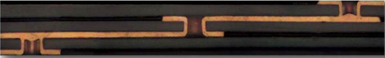
Many of today's flex PCB designs utilize the same high-density components found in rigid PCB designs. This requires the use of blind and or buried vias to allow the signal lines to be routed out from within the high-density components or the high-density areas of the design. The most common component that we see driving this today is the 0.4mm pitch BGA package.
Blind vias allow the signals to be dropped down to the next layer from within the BGA SMT pad and then routed out from there. In high pin count devices, additional blind and or buried vias may be required. Differences exist in how blind and buried vias can be implemented in a Flex PCB design due to the materials and manufacturing processes required.
Via-in-Pad for Higher Density blind via Flexible PCB
For flexible PCB designs with high layer counts utilizing high density outer layers, the extra area utilized for separate pads and SMT components severely limits the available space for trace fan out. By designing via-in-pad in flex and rigid-flex PCB, it can significantly increase density, utilizing vias as mounting pads. The copper- or silver-filled flat vias allow for soldering components directly on via holes.
Utilizing via-in-pad will release extra surface area for routing of traces. However, like any new technology, there are a few points to be aware of when using this type of construction with flex. When manufacturers fill rigid PCB vias for SMT pads, they are typically filled with a conductive epoxy, copper plated, and then planarized flat. The final sanding leaves a very smooth pad surface allowing the assembler to process the circuit board normally through the pick-and-place cycle.
The via-in-pad technology has progressed so that via fill is very common on rigid PCBs. The same equipment utilized on rigid PCBs to perform fill and planarization will crumple a flex panel. A flexible PCB panel will not be held stiff enough in the screen fill machine nor will it survive the screening fill process, which presses hard on the surface to drive the thick ink into the shallow hollow of the microvia. Also, the flexible PCB panel will bend and crinkle in the tough sanding planarization machine.
Rigid PCB vias are conductive ink filled after drilling and electroless plating, but before imaging and etching. After an oven cycle to cure the conductive ink, a sanding process is used to flatten the surface and remove any of the conductive fill material from the surface. The resulting surface is quite smooth and ready for dry film. The rigid panel has dry film applied, imaged, developed, and electroplated with copper plating and tin. The dry film is removed, the base copper etched, and then tin stripped. The resulting via surface hole is copper filled and is now reasonably flat copper with a slight dimple, if any.
The via fill operation for flexible PCB is quite different. It utilizes a horizontal, flat screen-printing process to fill the vias with conductive ink. Inevitably, some fill material, usually a small bump,is left on the surface of the panel where it is not wanted. This over-screening residue needs to be removed. The residue will be plated over during cap plating, resulting in a possible short when final etch is performed. It is very difficult to remove this unwanted residue on a flex PCB panel. They are too thin and crumple easily when run through a planar sanding machine, which is typically used to remove the hardened fill residue and a small amount of surface copper on a rigid PCB. Due to these difficulties, this method is seldom used on flex microvias or laser vias.
A new and improved process for a flat via-in-pad on multilayer flex PCB is to fill the vias with a special type of copper plating. On thin flex layers that are laser-drilled, the new copper fill plating chemistry is designed to fill the laser via from the bottom up, creating a reasonably flat top on the via. Though some small dimpling can usually be seen, it presents no problem for assemblers. This plating technology is used on a wide range of flex and rigid-flex PCB.
Top flex circuit manufacturers have specially designed copper plating lines which preferentially plate inside the via holes, effectively filling them without plating any significant amount of copper on the panel surface. Excess electroplated copper on the surface is not desired as it would be a less ductile copper where, typically, RA copper for the traces is required for flexibility. Also, any extra copper plating on the trace surface will make it very difficult to etch very small features on outer layers that are typically used on high density designs utilizing via-in-pad technology.
Because the vias are selectively fill-plated with only copper, and resin fill is not utilized, the surface is smooth enough to forgo a subsequent sanding operation. The entire sanding and conductive screening process with the uneven surface topography of the flex PCB is therefore not a problem. The only negative to the copper plating fill process is that the copper-filled vias are sometimes not completely filled flat or have a small outward dimple. The dents and small dimples are not a problem for the assembler. The use of filled copper vias in flex can greatly increases routing area by freeing up via pads and spaces.
16-layer blind via flex PCB for medical application
The high packing density with lots of BGAs requires a highly integrated printed circuit board with 16 layers and buried as well as blind vias. The numerous signals from the sensors are transmitted through 6 flex layers. In order to keep the 6-layer flex areas flexible bookbinder and window technology was used.
Hemeixin core competence lies in the production of highly complex HDI, high-frequency and high-reliability circuit boards for medical,defense, aerospace, industrial and semiconductor applications.
Due to long-term dedication and expertise, Hemeixin has earned a solid reputation for being a technology leader and the partner of choice for providing leading flex, rigid-flex and rigid ultra-HDI/microvia circuit boards solutions - custom tailored to the corresponding requirements.


