Semi-Flex PCB Manufacturing
Semi-Flex PCBs are a cost-efficient solution to optimize a great number of projects. Made from FR4 material, which is the most affordable base material for PCBs, it can reduce space, weight, and improve the reliability of the final product as connectors are considered a reliability risk in many applications.
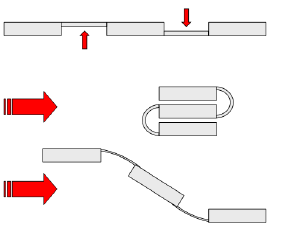
A semi-flex PCB is characterized by its ability to bend or flex to a certain degree while maintaining its structural integrity. This type of PCB is often used to save space in the final product and avoid the use of connectors between two circuit boards. Semi-flex PCBs are manufactured using a combination of traditional PCB fabrication processes, such as photolithography, etching, and drilling, as well as specialized techniques for handling the flexible substrate. The final product is a PCB that can bend or flex to a certain degree while maintaining its electrical performance and durability.
Semi-Flex PCB Technology Innovative Solutions for 3D Assembly
Hemeixin offers semi-flex circuit boards manufactured with conventional rigid FR-4 base materials. These boards are suited for one-time flex-to-install applications. The technology can be used for double-sided and multilayer boards. Because only standard materials and processing are used, this technology offers a low-cost alternative for applications with flexible or bendable areas in a printed circuit board (“PCB”). A semi-flex board most often replaces two PCBs and the required connectors and cables or allows a three-dimensional design and placement of the PCBs in a device.
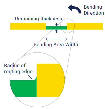
The flexible segment in a semi-flex PCB is generated by controlled depth milling of the PCB in the required area. Hemeixin’s newest routing machines with z-Axis technology and integrated measuring and mapping functions is critical to the consistent and high-quality fabrication of semi-flex.
Often layout designers are reluctant to upgrade from a standard PCB with connectors to a notoriously expensive rigid-flexible printed circuit. The advantages are immense, but so are the costs and the layout requirements compared to standard PCBs. Many times this "jump" from standard technology to a high-tech segment is not necessary. Many printed circuits do not require dynamic bending capabilities in operation but only need to be fit into the housing neatly. This is called a "flex-to-install" requirement and here semi-flex offers a really cost-saving alternative technology.
A semi-flex PCB, can only be bent in certain areas that have been made to flex. As a result, the PCB will only bend in predetermined ways and at defined points. With the exception of the flex areas, a semi-flex PCB is stiff and more akin to a traditional rigid PCB. This is because semi-flex PCBs are manufactured using the manufacturing process ‘controlled depth routing’ or ‘milling’ down the FR4 material on the PCB until it is extremely thin and flexible. The flexible section is then treated to prevent cracking, allowing it to bend more or less freely. Semi-flex PCBs can also be manufactured by using thin core laminates. Laminates as thin as .005 mil. are utilized for static flex applications. RA (rolled annealed) copper foils is recommended to prevent cracking and allow for a more robust flex.
Semi-flex PCBs are well-suited to situations in which a PCB must be bent only for installation and projected future maintenance. Their flexible nature also makes semi-flex PCBs a good design choice for applications in which space is a major consideration. Semi-flex PCBs can be found in many common applications. Automobiles, industrial equipment and even safety electronics make extensive use of this circuit board category.
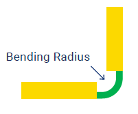
Hemeixin recommends a board or multi-board bar or frame to stabilize the bending area in assembly. The assembly process can be standard because no additional tempering, preparation, or handling is necessary. Installation of semi-flex circuits should be done with a bending tool to guarantee that the minimum bending radius is not violated.
Semi-Flex PCB Overview
- FR-4 material processing parameters
- The material in ‘bend-area’ is reduced in thickness by depth controlled routing
- Suitable for flex to install (1-time bend) applications only (no dynamic flex)
- No expensive flex materials and process-flow required
- One PCB replacing two PCBs + interconnects (connectors, solder-joints)
- PCB is mechanically fixed after bending
Semi-flex PCB advantages
- Size Optimization: Using FR4 Semi-Flex optimizes the PCB size, saving the space of the connectors on both “rigid” parts.
- Cost-Effective: The FR4 Semi-Flex replaces 2 or more PCBs, simplifies the assembly process, eliminates connectors, and is cheaper than the Rigid-Flex solution.
- Time Saving: FR4 Semi-Flex reduces the time needed for design, procurement, and assembly.
- Reliability and Durability: Fewer solder joints and fewer connectors.
To optimize transportation-safety and assembly, semi-flexible PCBs should always be produced in panels. You can easily seperate the prints from the panel after assembly and install the boards.
Semi-flex pcb design guidelines
|
Material (reference) |
IT-158, Autolad1, SB170G, EM 825 |
|
Methodology |
Z-Axis Routing / ZAR |
|
Depth control routing tolerance |
+/-75 μm (3mil) |
|
Bending Layer |
1 or 2 |
|
Bending Cycle |
Max. 5 (depending on design) |
|
Bending Radius |
Min. 22T (T=the remaining thickness) |
|
Bending Area Width(BAW) |
Min. 0.02 θR (θ=Bending Angle) |
|
Cu thickness on bending layers |
HOZ,1 OZ, 2OZ, 3OZ |
|
Trace width and spacing on the bending layers |
Min. 0.2mm for HOZ, 0.25mm for 1OZ |
|
Glass type |
Fine glass e.g. 106, 1080 |
Semi-flex pcb material minimum thickness
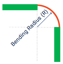
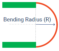
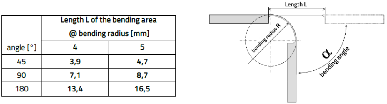
A minimum bending radius (R) needs to be taken into account because semi-flex is based on glass-reinforced rigid base material. The bending radius mainly depends on the ‘Remaining Thickness’ (RT) in the bend-area.
A guideline to calculate:
The minimum Radius (R): R = 22 * RT
The Bend Area Width (BAW) depends on the
Bending Angle (α) and Radius (R): BAW = (0.017 * α * R)
Example based on Remaining Thickness (RT) = 0.25mm;
R = 22 * 0.25 = 5.5mm
BAW = 0.017 * 90 * 5.5 = 8.4mm for 90˚ Bending Angle
BAW = 0.017 * 180 * 5.5 = 16.83mm for 180˚ Bending Angle
90° Bending Angle
180° Bending Angle
Before Bending
After Bending
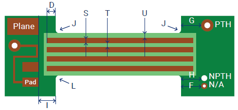
Bevel :0,4 x 45°
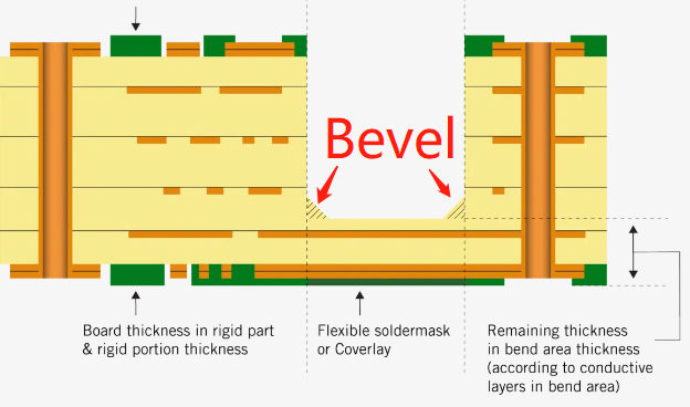
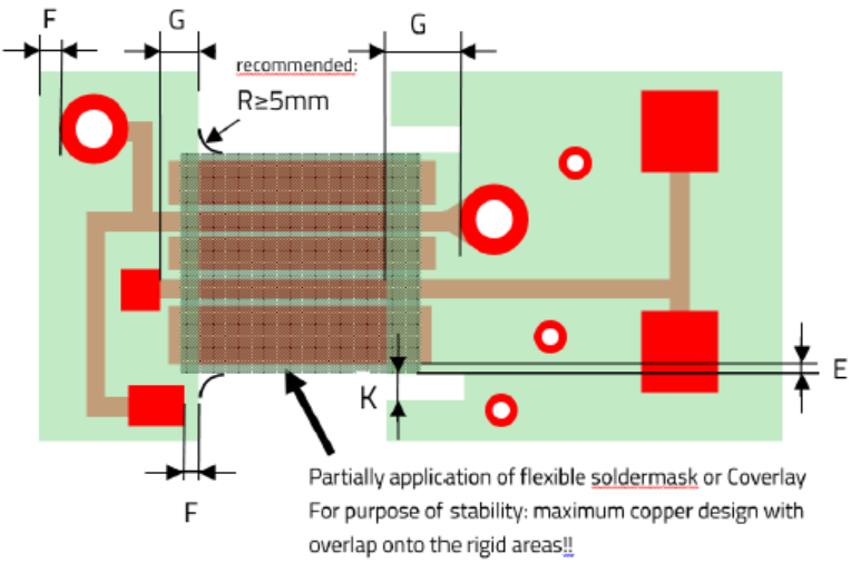
PCB radius≥5MM
Semi-Flex PCB (ZAR) design Rules
Side View
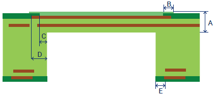
Top View
![]()
|
DESCRIPTION |
VALUE |
UNIT |
MARKED |
|
Minimum nominal thickness of bending area for one copper layer |
0.20 |
mm |
A |
|
Minimum nominal thickness of bending area for two copper layers (NOT Preferred) |
0.25 |
mm |
A |
|
Minimum flexible solder mask overlap onto solder mask |
0.50 |
mm |
B |
|
Minimum solder mask clearance from semi flex area |
0.15 |
mm |
C |
|
Minimum length of copper extending beyond the semi flex area (non functinal tracks) |
1.00 |
mm |
D |
|
Minimum rigid area copper clearance from semi flex area |
0.50 |
mm |
E |
|
Minimum microvia pad clearance from semi flex area |
0.50 |
mm |
F |
|
Minimum PTH pad clearance from semi flex area |
0.50 |
mm |
G |
|
Minimum NPTH clearance from semi flex area |
0.50 |
mm |
H |
|
Minimum component pads clearance from semi flex area |
1.00 |
mm |
I |
|
Minimum radii in the area of transition from rigid to semi flex area |
N/A |
mm |
J |
|
Minimum routing depth |
N/A |
mm |
K |
|
Minimum routing diameter |
N/A |
mm |
L |
|
Minimum track width (18μm) |
0.20 |
mm |
S |
|
Minimum track spacing (18μm) |
0.20 |
mm |
T |
|
Minimum track width (35μm) |
0.25 |
mm |
S |
|
Minimum track spacing (35μm) |
0.25 |
mm |
T |
|
Minimum track spacing to Semi Flex area side edge |
0.50 |
mm |
U |
Recommendations for semi-flex PCB design
- Calculation of Length “L” for semi-flex area
Necessary length L of the bending area is:
L = angle x radius R x Pi / 180° + 2 x 0.4mm (bevel Y)

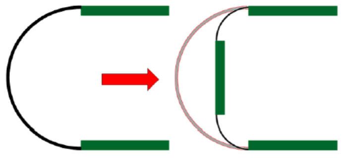
- 180° bending replaced by 2 x 90° with rigid middle part

- Fill up free areas in the bending area with hatched copper
- Design S-shaped bend accordingly with milling from two side!
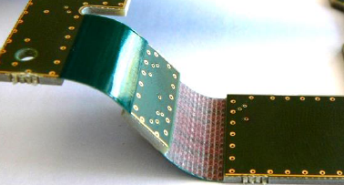
A Semi-Flex circuit is made by thinning a portion of a rigid FR4 PCB down to 0.1~0.2mm making it bendable up to a certain point. Because it is a mono-material, made only from FR4, Semi-Flex is a cheap alternative to complex Polyimide Rigid-Flex circuits. After populating, the semi-flex PCBs can be bent for the casing. It must be static use, not dynamic.
FR4 Semi-Flex is a cheaper solution than Rigid-Flex. It should not be used for applications exposed to shock and vibrations. FR4 Semi-Flex creates reliable 3D connectivity opportunities by replacing board-to-board connectors, which leads to space and weight reductions. It is widely used in Instrumentation, Metering, Sensor technology, and Industrial controls.


