PCB Design
- High speed digital PCB boards
- High frequency RF / Microwave PCB designs
- Low level analog PCB designs
- Ultra low EMI designs for MRI applications
- DDR2, DDR3, DDR4 memory designs
- Printed antenna designs
- Power Distribution
- HDI PCB boards
- Blind and buried vias
- ATE PCB boards
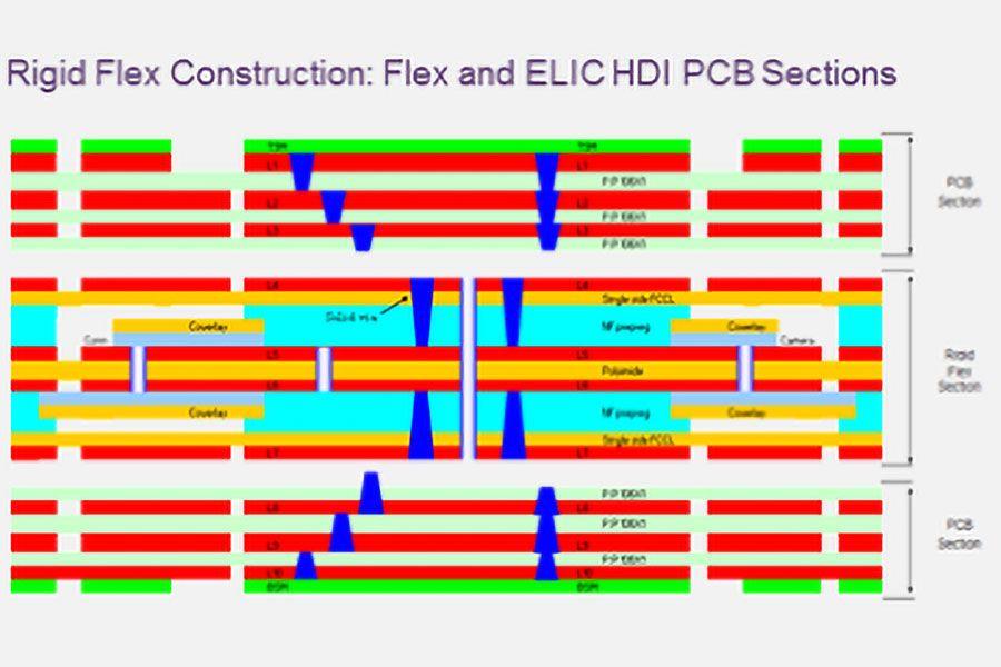
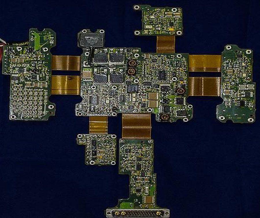
- Flexible PCB boards
- Rigid-flexible circuits
- Up to 16 GHz
PCB Design Tools
- Allegro, Pads, Mentor Expedition, Altium Designer
PCB Design Package Types
- BGA, uBGA, CSP, QFP, QFN, TSSOP, TQFP, SOIC
PCB Design Schematic
- CIS/ORCAD, Concept-HDL, Montor DxDesigner, Design Capture, etc.
Hemeixinpcb believes in courteous, swift and professional customer service. The company’s goal is to provide rapid and high-quality solutions to the satisfaction of all customers – both new and old. Many years of experience, use of advanced technologies, compliance with the requirements of IPC standard, and a team of highly experienced and knowledgeable designers that plan every step in advance – all these shorten the fabrication time and TTM (Time to Market).
PCB Design - With varied production technologies
- RIGID Multilayer / Motherboards/Backplanes / All Types IAW IPC2221+IPC2222
- Flexible / Rigid-Flex PCBs In-Accordance-With IPC-2223
- MicroVias / Stacked & Staggered & Blind & Buried Vias IAW IPC2226
- HDI= High Density Interconnect IAW IPC2226
PCB Design Capability
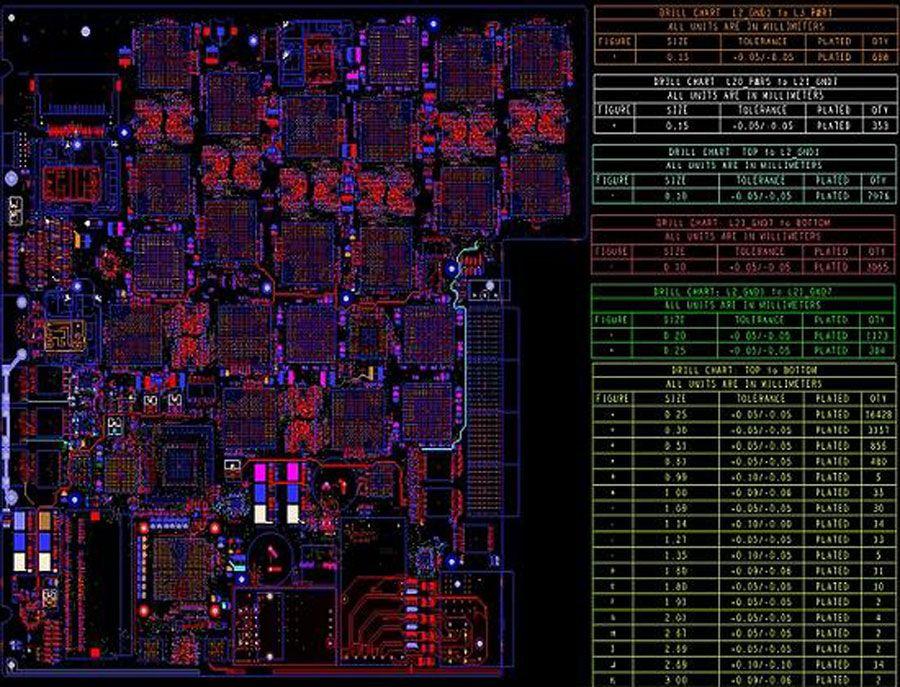
- Highest layers::60 Layers
- Maximum PIN count:69000+
- Maximum connections:55000+
- Minimum line width:1.5mil
- Minimum line spacing:1.5mil
- Minimum via:6mil(3mil laser hole)
- Maximum BGA in a single PCB:62
- Maximum BGA PIN spacing:0.4mm
- Maximum BGA PIN count:2597
- Highest speed signal:28Gbps
- HDI PCB design: 1+N+1, 1+1+..+1+N+1+1+..+1, M+N+M Stacked Microvia and Any layer HDI PCB up to 30 layers.
Required information to quote pcb design & Layout
- Complete and verified schematic(s) in one of the software platforms we offer: PCAD, Cadence Allegro, PADS (Mentor Graphics), or Altium Designer.
- Complete and verified BOM. Customer must spec. out each component for the layout, based on their familiarity with requirements of the circuitry.
- Part numbers for components must be complete, along with package/footprint details for each component.
- Board form factors (Dimensional details, board thickness, tooling hole locations, mechanical constraints, etc.) in one of the software platforms we offer, listed above. We can also work with DXF files from CAD tools (like AutoCAD, etc.). Also provide details on: surface finish, solder mask, silkscreen, finished copper weight, etc.
- Any special layout routing or fabrication requirements. Special Requirements or Non-Standard Tolerances.
- Is the board to be RoHS compliant, Yes or No?
PCB Design process flow chart
To assist our clients with better time-to-market and control on product development, a special design process flow has been implemented by the Hemeixinpcb.

High Speed PCB Design Capabilities
Due to the high speeds of many electronic designs in modern technologies, the physical characteristics of the design-implementation (PCBs, packages, interconnects, etc.) contribute to the behavior of the circuits just as much as the parts of the electrical design that are included in the schematic.
Today, every digital circuit board runs at high speed. We build the advanced high speed electronics companies rely on to build competitive digital products. As high speed PCB experts, we designand manufacture complex digital systems that push the limits of modern electronics. We target advanced applications that other firms struggle to design and build, and we’ll ensure your new system will be fully manufacturable at scale.
- Dense, high-layer count, high speed layout and routing expertise
- Layout and routing for standard high-speed digital interfaces: DDR3/4/5, mulit-Gbps SerDes, PCIe, MIPI standards, etc.
- Aggressive form factor, lower layer count PCBs with multiple high speed interfaces
- Stackup construction and DFM expertise for high speed digital products
- Mixed-signal layout in products with wireless protocols
RF PCB Design Capabilities
RF PCB design (Radio Frequency printed circuit board design, RF printed circuit board design) is one of the most exciting application for electronics designers today, any smartphones, sensors, robotics, and security systems are in demand of complicated and high frequency boards, which will require RF PCB design. The greater complexity of circuitry also brings greater headaches for RF PCB designers, Hemeixinpcb RF PCB design team are here to help!
RF PCB (also named Radio frequency PCB or Radio frequency printed circuit board)and Microwave PCB, is designed to operate high frequency signals with small wave length, surely related to radio frequency, The laminate materials for RF PCB design contains very specific characteristics, such as dielectric constant (Er), loss tangent, and CTE (co-efficient of thermal expansion), these laminates have more advanced composites compare to normal FR-4 material.
IEEE standard designate RF(radio frequency) is from 20KHz to 300GHz, and Frequencies ≥ 1 GHz are called microwave(1MHz=1000KHz,1GHz=1000MHz), This is roughly between the upper limit—audio frequencies and the lower limit —infrared frequencies.
In PCB industry, however, any high frequency PCB design that operates above 100MHz are considered as RF PCB design, and any PCB operates above 2GHz we call it a Microwave PCB.
Today's advanced electronics integrate multiple protocols and run at higher frequencies than ever before. As RF PCB design experts, we've built complex systems with multiple wireless protocols and digital circuit blocks, and we’ll ensure your new system will be fully manufacturable at scale.
- High resolution long-range and short-range radar
- PCBs with unique interconnects, emitters, and resonator structures
- Cascaded and MIMO mmWave sensors and systems
- IoT products and embedded systems with multiple wireless protocols
- RF power systems, including power supplies, amplifiers, and power-over-RF
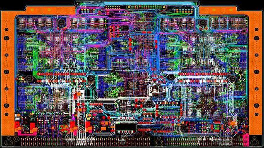
HDI PCB Design Capabilities
Large-scale integration in HDI PCB layout involves multiple low-speed and high-speed digital protocols, as well as a cleear focus on best DFM practices to ensure high-yield production. We adopt a production-first mindset when floorplanning your design, and we'll ensure your high-density PCB layout meets the needs of advanced applications.
- HDI PCBs with multiple digital protocols (DDR, PCIe, SerDes, LVDS, etc.)
- High-density double-sided designs with multiple BGAs
- System-on-module (SOM)/computer-on-module (COM) and baseboard designs
- High layer (26+) count backplanes and daughtercards
HDI PCB designs carry important material requirements and component selection considerations that are not found in many other systems. Once your new design has passed review and is ready for production, we’ll engage with our manufacturing partners to get your design through production and bring you the most value:
- HDI stackup design - An HDI stackup will be a major determinant of successful manufacturing and solvability in an HDI PCB layout. Layer counts, routing/via style, and HDI material selection must be qualified with a manufacturer before the design begins.
- Floorplanning - HDI systems generally involve at least one BGA with high ball count and fine pitch. BGAs, high pin count connectors, peripherals, should be placed early to ensure a coherent plan for routing that does not require addition of new layers late in the design phase.
- Interconnect design - Stackup design is related to transmission line design for any high-speed impedance-controlled protocols in an HDI PCB. Interconnects must be designed while to hit impedance and loss targets while accounting for skew constraints, flight times, and routing paths in an HDI PCB stackup.
- Via design - Manufacturable and reliable via design is critical in HDI PCBs. This will also influence the stackup design choices as vias require specific material and thickness choices to ensure manufacturability and reliability.
HDI PCB design starts with a manufacturable stackup that can meet your routing needs, as well as your impedance and loss targets. Standard HDI stackups with via/microvia placement and layer access capabilities are provided by hemeixinpcb.


