
Flex-Rigid PCB design issues
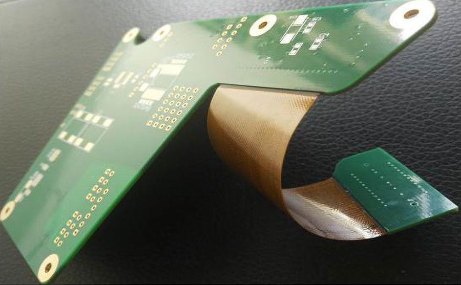
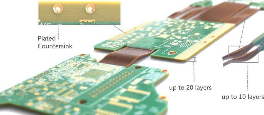
Rigid-flex is the ideal solution for applications with multiple rigid PCBs having SMT components on both sides and requiring interconnects between the rigid PCBs.
The most familiar products are probably smartwatches that link with smartphones, and fitness trackers that are also worn on the wrist. But beyond these consumer products, wearables have made huge inroads into medical devices and military applications. Now, smart clothing is appearing that could virtually eliminate the possibility of incorporating rigid PCBs. So what is required to successfully design flex and rigid-flex PCBs to keep up with the market?
Before designing a rigid-flex circuit, make certain that it is truly what you need. If the circuit only has a few layers, stiffeners are a less expensive alternative to rigid-flex pcb.
It is most cost effective to build a rigid-flex with an even number of layers. All rigid portions of the circuit should have the same number and stack-up of layers.
The biggest problem with designing rigid-flex hybrid PCBs is making sure everything will fold in the right way, while maintaining good flex-circuit stability and lifespan. The next big problem to solve is the conveyance of the design to a fabricator who will clearly understand the design intent and therefore produce exactly what the designer/engineer intended. Rigid-Flex circuit boards require additional cutting and lamination stages, and more exotic materials in manufacturing and therefore the cost of re-spins and failures are very much higher than traditional rigid boards. To reduce the risk and costs associated with rigid-flex design and prototyping, it is desirable to summary the rigid flex pcb design isusses to ensure correct form and fit. In addition it is necessary to provide absolutely clear documentation for manufacturing to the fabrication and assembly houses.
1.Rigid Flex PCB Board basic specification.
- A part number (including revision number) for your design to ease tracking
- Board thickness (.including flex part thickness, each stiffener area’s thickness and rigid part total thickness).
- Type of board material (Polyimide adhesiveless base material or Polyimide adhesive base material, FR4, high-temp FR4, Rogers, Teflon, etc etc). Polyimide adhesive base material and FR4 is standard
- Number of layers
- Surface finish (OSP, immersion gold, etc). Immersion gold is standard
- The color for solder mask and coverlay. Yellow coverlay and Green is standard
- Copper weight on outer layer (1 oz., 2 oz., etc). 1 oz. is standard
- Copper weight on inner layers (.5 oz., 1 oz.). Either is standard
- Stiffener material and thickness( FR4, Polyimide, Stainless steel, copper, ect)
- The minimum trace and space widths in your design
- Indicate your board dimensions on a mechanical layer
- Do you want your boards to remain panelized, or supplied individually cut?
- Gerber files, drill files, IPC-356A (optional)
2.Via placement
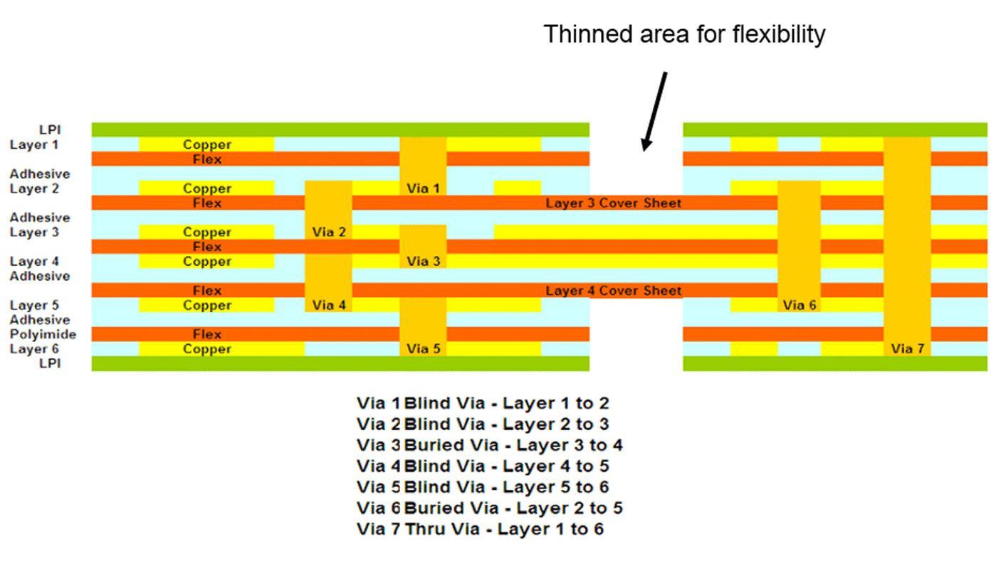
For multi-layer flex areas, it may sometimes be necessary to place vias to transition between layers. If possible it’s recommended not to place vias, as these can suffer fatigue rapidly in flexing movement. It is also necessary to keep at least 35 mils clearance between the copper annulus of the nearest via to the rigid-to-flex board interface. Board edge clearance rules can take care of this automatically in the PCB CAD editor.
As for the need to place vias – if you must have vias in a flex circuit, use “rooms” to define regions where you know there will be no bends and use the PCB editor’s design rules to allow via placement only in those stationary areas. An alternative is to use the layer stack manager to define “rigid” sections that are ultimately flex but with a rigid dielectric stiffener material adhered to them.
3.Define the stack by area
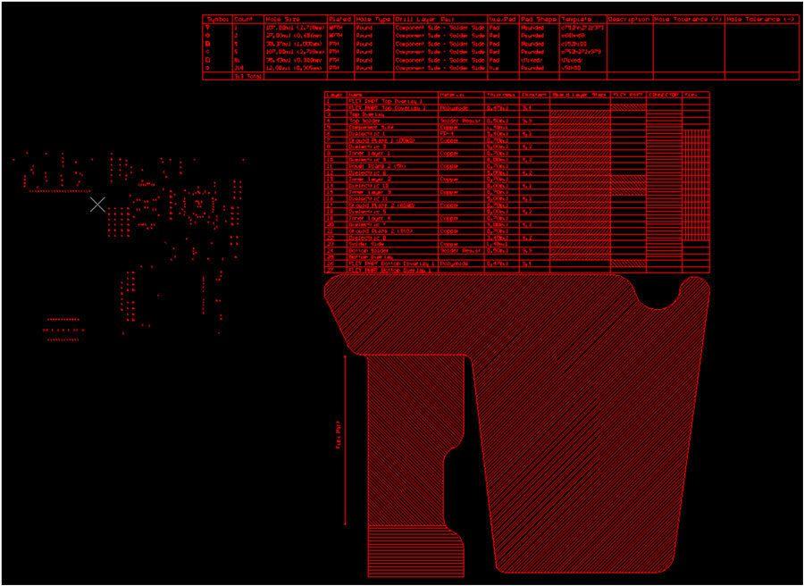
The most important documentation you can provide your fabricator is arguably the layer stack design. Along with this, if you’re doing rigid-flex pcb, you have to provide different stacks for different areas, and somehow mark those very clearly. A simple way to do this is make a copy of your board outline on a mechanical layer, and lay down a layer stack table or diagram with a pattern-fill legend for the regions containing the different layer stacks.
4. Define the drill by layer
The most important documentation you can provide your fabricator is arguably the drill information. Along with this, if you’re doing any layer rigid-flex or Blind and buried vias rigid flex pcb, you have to provide different drill data and drill information for different layers, and somehow mark those very clearly. A simple way to do this is make a copy of your board layer stack and insert drill holes’ diagram with a pattern-fill legend for the drill information.
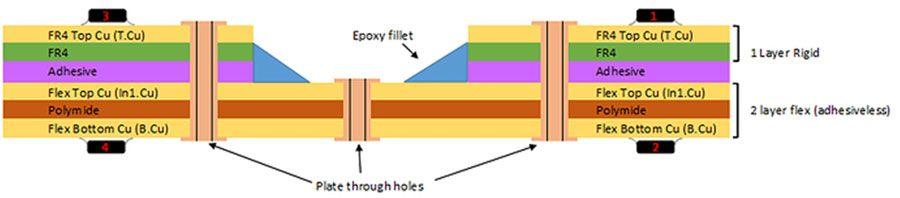
5.Adhesive Fillets (In Transition Zone)
For rigid-flex printed circuit boards (PCBs), the space joining rigid material to flex material (Transition Zone) sometimes contains imperfections that, although acceptable, could impact effectiveness of the final part. Transition zone imperfections can include any of the following:
- Adhesive squeeze-out
- Protruding dielectric materials
- Crazing
- Haloing
In “rigid/flex” type circuits and circuits which require a rigidized stiffener, the area where the flexible section intersects the rigid section is called the transition zone. This zone generally contains material edges that are not smooth. These rough edges can cause damage to the conductor paths if the flex circuit is bent sharply against them. To prevent this from occurring, it is highly recommended placing a bead of an epoxy material at this transition area. As shown in the illustration below.
6. External Layer Copper or pads to Flex Transition Zone min. spacing = 0.040”
As measured flex transition zone(s) and external layer copper or pads distance less than 40 mils. Ensures sufficient spacing to allow for reliable external layer imaging processing.Rigid layers, while in production panel configuration and prior to final lamination process, are required to have the flex areas removed. This creates in internal edges, created by the height difference between the rigid area and the flex area, which the external layer image transfer films must transition.
If you have any questions or concerns with your rigid-flex PCB board, we’d love to hear from you! Feel free to reach out to us during the design stage, our engineers are always ready to help.


