HDI PCB - High Density Interconnect PCB Design and Manufacturing
High Density Interconnect PCB Design and Manufacturing
High-density interconnect, or HDI, circuit boards are printed circuit boards with a higher wiring density per unit area than traditional printed circuit boards. In general, HDI PCBs are defined as PCBs with one or all of the following: microvias; blind and buried vias; built-up laminations and high signal performance considerations. Printed circuit board technology has been evolving with changing technology that calls for smaller and faster products. HDI boards are more compact and have smaller vias, pads, copper traces and spaces. As a result, HDIs have denser wiring resulting in lighter weight, more compact, lower layer count PCBs. Rather than using a few PCBs in a device, one HDI board can house the functionality of the previous boards used.
High-Density Interconnect (HDI) is simply a PCB with more number of interconnections, occupying minimal space. This results in the miniaturization of the circuit board. The components are placed closer and the board space is significantly reduced but the functionality isn’t compromised.
As per IPC-2226, high-density interconnect (HDI) boards have a higher wiring density per unit area than conventional PCBs. Thus to achieve this, as a designer you need to opt for smaller vias, smaller traces, and fewer layers.These PCBs have components packed in a small space to achieve the required formfactor.
These PCBs use different via technologies like microvias, blind and buried vias,and built-up laminations. Implementation of this, frees up space foradditional components and offers more routing versatility.
Hemeixin is one of the first companies to provide volume high density interconnect PCB capability to our customers. Our continuous investment in developing world-class, fine-line Microvia technology has made us a leading Microvia HDI PCB board manufacturer. Our through experience and commitment in providing a complete solution for our customers helps to resolve early HDI PCB design issues, shorten the lead time, and deliver a high-quality, cost-efficient product.
Our HDI PCB manufacturing includes:
- Any layer hdi pcb technology
- Skipped, telescopic, stacked μvias
- Copper filled via, HDI via fill plating, via in pad technology
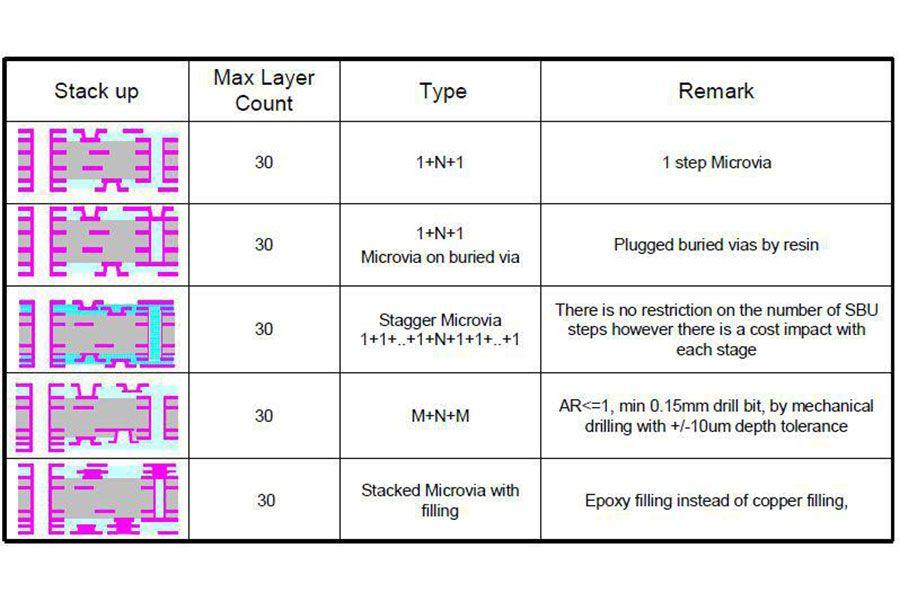
- HDI PCB build up: 1+N+1 HDI PCB, 2+N+2 HDI PCB, 3+N+3 HDI PCB, 4+N+4 HDI PCB, Up to 9+N+9
- Low loss pcb material (I-Speed material, FR408HR, Megtron4, EM-888, N4000-13EP, N4000-13, TU-863+, TU-872lk, TU-872SLK, TU-872SLK SP etc)
- High Speed Digital PCB laminate: (I-Tera MT40 / RF, Tachyon-100G, Megtron6/R-5775, TU-883, TU-883SP, IT-968, IT968SE etc)
- RF PCB, Microwave pcb laminate: (RO4450F, RO4350B, RO4835, RO4003, RO4533, Taconic TLY series, TLY-5, RF35, TSM-DS3, Astra MT77, RT/Duroid 5880, RO3203, RO3003 etc)
- Sequential Lamination
- Stacked Microvias
- Blind & Buried Vias
- Laser Direct Imaging
- 0.05mm Trace/Space
- Fine Pitch (Down to 0.3mm)
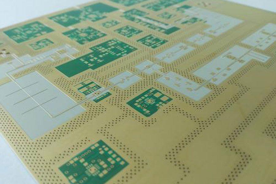
Overview HDI PCB fabrication capabilities:
|
Manufacturing considerations for HDI printed circuit boards
- Number of laminations: The number of laminations used in the stack-up is the most important factor when it comes to HDI manufacturing.This in turn decides the cost of the overall board.
- Choosing laser drilling over mechanical drilling: Laser-drilled vias will reduce cost, time, and are effective for controlled depth vias.
- Aspect ratio of laser drill: The aspect ratio of the drilled vias should be smaller for easy plating and good thermal properties. This is achieved by choosing microvias that generally have an aspect ratio less than 1. The ideal value is 0.75:1.
- Drill-to-copper: Drill-to-copper is defined as the distance between the edge of a drilled hole and the nearest copper feature. Design automation tools do not take into account the drill-to-copper clearance. While designing for HDI, the drill-to-copper capability of a manufacturer needs to be considered. The typical value of drill-to-copper clearance is 7 to 8 mils.
- Landless via technology: Using laser drilling, it is possible to drill vias with no pads at all. This is called landless via technology. Implementing this technology reduces the size of the board even more.
- Choosing the right surface finish: ENIG or ENEPIG surface finishes are preferred over hard or soft gold for high-density boards.
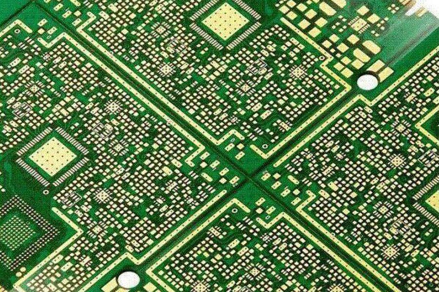
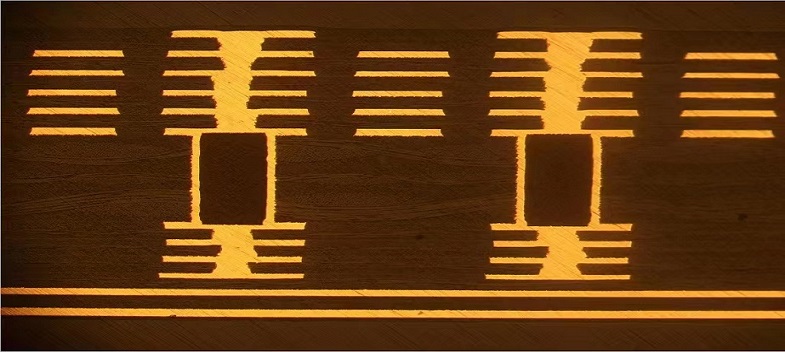
Microvias HDI PCB manufacturing samples
HDI PCB Board Design and Manufacturing Processes
HDI PCB Board Design
There are a number of steps involved in the typical PCB manufacturing process, but HDI PCB manufacturing uses some particular steps that may not used in other boards. The HDI board design process starts like many other processes, where the
- Determine the layer count required to route all signals, either by using the largest BGA component on the board or by using the interface + direction count from the largest IC on the board.
- Contact your HDI PCB fabrication house to select materials and obtain dielectric data to create your PCB stackup.
- Based on layer count and thickness, determine the via style that will be used to route signals through inner layers.
- Perform a reliability assessment if relevant, to verify that the materials will not stress interconnects to fracture during assembly processing and operation.
- Determine design rules based on fabricator capabilities and reliability requirements (need for tear drops, trace widths, clearances, etc.) to ensure reliable manufacturing and assembly.
Stackup creation and determination of design rules are the critical points as they will determine ability to route the board and reliability of the end product.
HDI PCB Design DFM Requirements
Although DFM requirements relating to clearances in an HDI PCB are quite stringent, these can be accommodated by taking advantage of your design rules in your PCB design software. Some of the important DFM requirements to gather before layout and routing include:
- Trace width and spacing limits
- Annular ring and aspect ratio limits, especially for high reliability designs
- Material system used in the board to ensure controlled impedance in the required stackup
- Impedance profiles for the desired stackup or layer pairs if available
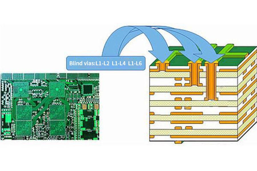
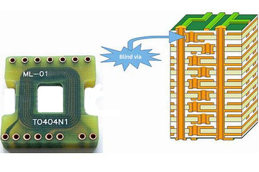
- Blind vias connect an exterior layer to at least one interior layer without penetrating the entire board.
- Buried vias connect one or more inner layers together without any connections to the exterior layers of a board.
- Any layer HDI (or ELIC) refers to the use of stacked copper-filled microvias to connect multiple layers in a PCB.
HDI PCB design tips
Once you determine that you require HDI, you need to look at the stack-up. Don’t use more than three sequential layers unless there is absolutely no other solution. It is recommended that you use a good fanout strategy for complex ICs, like BGAs and QFNs – this will help you reduce the number of sequential laminations if you plan your fanout strategy properly.
Smart component selection
Usually, an HDI board contains SMD (high pin count) and BGA (≤ 0.65 mm) components. The spacing/pitch between their pins should be chosen wisely since it helps to define trace widths, via type, and board stack-up.
Use of microvias
Use microvia or sequential build-up technology (< 0.15 mm diameter). It can help you to achieve twice the number of pins/area than through-hole pins. These microvias are used to form the escape area of dense components (high I/O, micro BGA). The low inductance of microvia makes them suitable for high-speed applications, for connecting power planes with a decoupling capacitor, and where noise reduction is required.
Material selection
Material selection is important for every circuit board design. But we must say it is more important for HDI boards. The designer’s goal is to select the right material for manufacturability, at the same time, meet the temperature and electrical requirements. Thep hysical thickness of the material is important when considering the aspect ratio of the microvia to be plated.
Capping of vias
Always fill/cap the microvias to provide a planar copper surface. It also allows easy placement of active parts on both sides of the board. Ignoring this will result in air bubbles and will cost you in the solder joint quality.
An offset microvia grid
It allows via-in-pad design. Such microvias can be centered in, offset from, or tangent to surface mount pads to provide extra routing.
Reduced plane perforation
Larger power/ground copper area under BGA improves power integrity (PI) and EMC. Wherever microvias perforate a plane; they create a very small gap with minor effects on SI, PI, and EMC. Perforate less to achieve improved image plane effect and higher shielding effectiveness.
Stack-up issues in HDI PCB design
Different layer materials have different CTE values and rates of moisture absorption, which triggers the possibility for delamination. Board designers can avoid it by using the same material for every layer or material with the same CTE value.
Testing
Functional or JTAG test methods are used for HDI PCB design rather than ICT. ICT is definitive but requires full nodal analysis. In the case of BGA that uses blind and buried microvias, you don’t have accessibility unless you bring these to the outer layer(that will violate the signal integrity). If you are using a small-pin package, then you might not have enough space for that.
Thermal management
To provide better thermal management for your design, refer to IPC-2226, which involves thermal issues. Designers need to be more concerned about the thermal issue as the component density of the HDI circuit is high. The thinner dielectrics that go with microvias are an aid to thermal dissipation. In order to maximize the dissipation, consider adding thermal vias.
Wiring demand vs. substrate capacity
Wiring demand is the total connection length required to connect all the parts in the board. The substrate capacity is the wiring length available to connect all the components. The substrate capacity should be larger than the wiring demand so that there will be enough capacity for wiring to complete the design with minimum cost.
Printed Circuit board density
Calculate the PCB density to measure the complexity of the design. The amount of density of a printed circuit board (Wd) asmeasured by the average length of traces per square inch including all signal layers.
The PWB density was derived by assuming an average of three electrical nodes per net and the component lead is a node of a net.
PWB Density (Wd) =β √([Cd] )×(Cc)
=β √([(parts per sq.in.)] )×(ave.leads per part)
Where:
Cd = component density = ave. parts per sq. inch for a design
Cc = component complexity = ave. leads per part
β = Constant, 2.5 for the high analog/discrete region, 3.0 for the analog/digital region, and 3.5 for the digital/ASIC region.
To be more precise, a PCB with an average of 120 to 160 pins per square inch is considered as an HDI PCB. The HDI design incorporates dense component placement and versatile routing. The HDI popularized microvia technology. A denser circuitry is crafted with the implementation of microvias, buried vias, and blind vias. The drill to copper is reduced in an HDI design.
Earlier in conventional board design, to add more components, more layers would have to be introduced. Also, only one type of connectivity was available.But with the emergence of HDI, more sub-connectivities are introduced between layers. This reduces the number of layers and makes the boards more compact. Compact boards with reduced thickness will have a smaller aspect ratio and increased reliability. These boards have thinner trace width and a reduced drill-to-copper ratio. Due to the short distance connections and lower power requirements, the signal integrity of these boards are better than conventional PCBs. You also can learn more about how to reduce HDI PCB cost.
HDI PCBs have a higher circuitry density per unit than conventional PCBs. They use a combination of buried and blind vias, as well as microvias — those that are 0.006″ or less in diameter. High-density circuit boards are PCBs with one or more of the following features:
- Through vias and buried vias
- Through vias from surface to surface
- At least two layers with through vias
- Coreless construction with layer pairs
- Passive substrate constructions that have no electrical connection
- Alternative constructions of coreless builds with layer pairs
Lamination & Materials For HDI PCB Board Manufacturing
Advanced multilayer technology allows for designers to sequentially add additional pairs of layers to form a multilayer PCB. The use of a laser drill to produce holes in the internal layers allows for plating, imaging and etching prior to pressing. This added process is known as sequential build up. SBU fabrication uses solid filled vias allowing for better thermal management, a stronger inter connect and increasing the board's reliability.
Resin coated copper was developed specifically to aide with poor hole quality, longer drill times and to allow for thinner PCBs. RCC has an ultra-low profile and ultra-thin copper foil that is anchored with minuscule nodules to the surface. This material is chemically treated and primed for the thinnest and finest line and spacing technology.
The application of dry resist to the laminate still uses heated roll method to apply the resist to core material. This older technology process, it is now recommended to preheat the material to a desired temperature prior to the lamination process for HDI printed circuit boards. The preheating of the material allows for better a steady application of the dry resist to the surface of the laminate, pulling less heat away from the hot rolls and allowing for consistent stable exit temperatures of the laminated product. Consistent entrance and exit temperatures lead to less air entrapment beneath the film; this is critical to the reproduction of fine lines and spacing.
Lamination process and the different types of HDI PCB stack-ups
HDI PCBs are multilayer boards that are constructed with densely routed layers. The boards are held together through lamination process and the layers are electrically interconnected using different types of vias.
The process of lamination begins with the etching of the inner copper layers. Later they are separated by partially cured laminates and stacked like a book with layers of prepreg on the top and bottom. The stack-up is then pressed and heated enough to liquify the prepreg. These liquifi ed prepregs cool down and stick the layers together.
For blind and buried vias stack-ups the PCB will undergo several numbers of sequential laminations. The more the number of laminations, the costlier will be the board.
To increase routing density, designers increase the number of layers, producing a complex stack-up. Manufacturers use sequential lamination processes to fabricate such complex designs.
Some of the common types of HDI PCB stack-ups are mentioned below:
- 1+N+1 – PCBs contain 1 build-up of high-density interconnection layers: This is the simplest HDI PCB design structure suitable for BGA with lower I/O counts. It has a fine line, microvias and registration technologies capable of 0.4 mm ball pitch, excellent mounting stability and reliability, and may contain copper filled via. It is a qualified material and surface treatment for a Lead-free process. Some of the examples include a Cell phone, UMPC, MP3 Player, PMP, GPS, Memory Card, etc.
- i+N+i (i≥2) – PCBs contain 2 or more build-up of high-density interconnection layers. Microvias on different layers can be staggered or stacked : This is a moderate complex HDI design structure that contains 2 or more build-up of high-density interconnection layers which allow the conductors on any layer of the PCB to be interconnected freely with copper filled stacked microvias structures. These structures are commonly seen in challenging designs that demand high-level signal transmission performance. They are suitable for BGA with smaller ball pitches and higher I/O counts and can be used to increase routing density in a complicated design while maintaining a thin finished board thickness. Some of the examples include smartphones, PDA, game consoles, and portable video recording devices.
- i+bN+i (i≥2) – Includes buried vias : Buried vias connect one or more inner layers together without any connections to the exterior layers of a board.
- Any layer HDI – All the layers of a PCB are high-density interconnection layers. This allows the conductors on any layer of thePCB to be interconnected freely with copper fi lled stacked microvia structures :This is the most complex HDI PCB design structure where all the layers are high-density interconnection layers which allow the conductors on any layer of the PCB to be interconnected freely with copper filled stacked microvias structures. This structure provides a reliable interconnect solution for highly complex large pin-count devices, such as CPU and GPU chips utilized on handheld and mobile devices while producing superior electrical characteristics. Some of the examples include smartphones, ultra-mobile PC, MP3, GPS, Memory cards, and small electronic devices.
HDI PCB Stackup Types
HDI PCBs come in a few different layout options. Some of the most common are 1-n-1 PCB and 2-n-2 PCB. A 1-n-1 PCB contains a single build-up of high-density interconnected layers, so it’s the “simplest” form of HDI printed circuit board. It requires one sequential lamination on each side of the core. The 2-n-2 PCB has two HDI layers and allows microvias to be staggered or stacked across layers. Complex designs usually incorporate copper-filled stacked microvia structures. Structures can climb to very high X-n-X levels, though complexity and cost typically limit the buildup. Another important option is the any-layer HDI. This involves an extremely dense HDI layout so conductors on any given layer of the PCB can interconnect freely with the laser microvia structures. These designs appear in GPU and CPU chips in smartphones and other mobile devices. Please link here to learn more about types of HDI PCB stackup.
i+N+i HDI PCB Stackup
More generally, this structure is known as an i+N+i stackup, where the outer sections consist of i sequentially laminated layers connected with microvias. The inner portion of the layer stack is connected to the outer sections at the top and bottom ends with a buried via, and the buried via portion (called a core via) also connects to the other inner layers. You could conceivably use any number of sequentially laminated layers on the outside of the stackup as long as it can be produced by hemixin pcb fabrication house. For example, 3+N+3 and 4+N+4 layer stacks are also common options provided by HDI PCB fabrication houses.
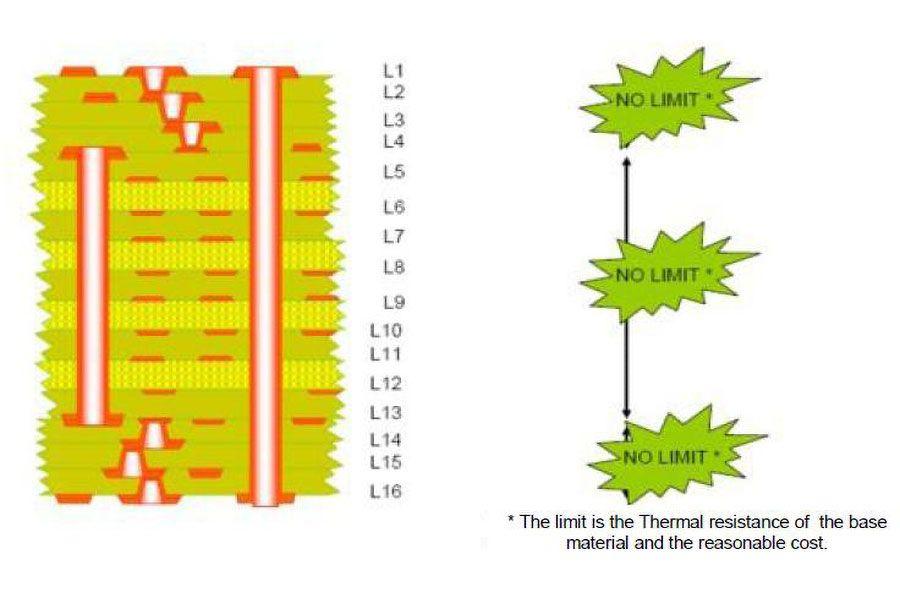
Also, there is technically no limit to N in theory, although practically this will be limited depending on the outer layer thickness and the total layer count. The reliability issues (to be discussed more below) found in microvia stacks is not present on this inner layer as a mechanically drilled through-hole is used to connect the inner layers before lamination with the outer layers. This forms a buried via once the entire stackup is built up. Once the stackup is built up, through-holes can also be placed in the finished layer stack going between all layers using standard drilling and plating processes.
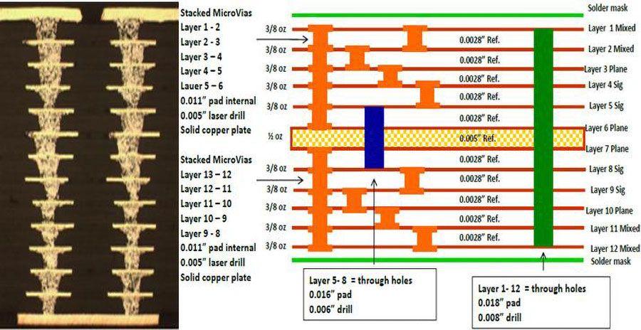
2 N 2 HDI PCB Stackup
The structure of a 2+N+2 PCB layer stack structure is defined in the IPC-2226 standards (known as Type III); this structure is shown below. This diagram is an exploded view of the layer stack to show the number of sequential laminations in the top/bottom portions of the stackup, as well as the buildup process for this PCB stackup. The top layers are the HDI routing layers, where microvias are used on thin dielectrics to access the interior layers in the stackup. The “2” in 2+N+2 refers to the fact that two sequential lamination steps are needed in the PCB stackup so that the two upper HDI layers can be stacked on the inner layer section.

Any layer HDI PCB stackup
Under the IPC-2226 standards, there are several standard PCB stackups used to support HDI PCB rouitng, which then allows trace routing into fine-pitch BGA components. Most of the standard HDI PCB stackup constructions use a core (buried) via, and/or a through-hole via touching all layers. Standard HDI PCB stackups might also use skip vias on the surface layer in addition to standard blind/buried microvias in order to allow BGA breakouts to access the inner layers of a PCB.
With PCBs containing even more layers and becoming thinner than ever before, new techniques are used to increase interconnect density. The most complex HDI PCB routing and stackup design style in use today is called every layer interconnect (ELIC). This routing style follows a simple idea: extend microvias throughout the entire PCB stackup so that signals can route on high density interconnects between any set of layers in the PCB. This might sound like an innocuous allowance, but it places constraints on the manufacturing process and material sets used to build the PCB.
ELIC is sometimes referred to as any-layer HDI, meaning signals can be routed on high density interconnects between any layer in the stackup. These advanced HDI PCBs contain multiple layers of copper-filled stacked in-pad microvias that enable even more complex interconnections. When using ELIC on an HDI board, each layer has its own copper-filled, laser-drilled microvias. ELIC uses only stacked copper-filled microvias to make connections through each layer. This allows connections to be made between any two layers in the PCB once the layers are stacked. Not only does this offer an increased level of flexibility, but it also allows designers to maximize interconnect density on any layer.
The image below shows a side cross-sectional view of an ELIC PCB HDI stackup. This microsection image contains stacked microvias throughout the PCB stackup, but it could also contain staggered microvias in different regions.

Through-hole vias are not needed anymore since all connections between the board are fabricated in the initial buildup. Since ELIC uses a copper-filled structure, plating techniques for filled vias (e.g., VIPPO) are not required. This particular stackup goes against the IPC warning on microvia reliability as we have stacked microvias spanning across the entire PCB stackup. Not all fabricators that can guarantee yield for ELIC PCBs without latent defects from reflow. Be careful when selecting a manufacturer that can provide these guarantees and be sure to implement their DFM rules to ensure your board will pass quality and acceptance criteria.
Laser Drill & Laser Direct Imaging: Technology for High Quality HDI PCB Manufacturing
High density interconnect PCB designs push the limits of technology and Hemeixinpcb is at the forefront of innovation, satisfying the most rigorous requirements.
Drilling the smallest of micro vias allows for more technology on the board's surface. Using a beam of light 20 microns (1 Mil) in diameter, this high influence beam can cut through metal and glass creating the tiny via hole. New products exist such as uniform glass materials that are a low loss laminate and low dielectric constant. These materials have higher heat resistance for lead free assembly and allow for the smaller holes to be used.
The demand for HDI PCB manufacturing has been increasing due to the advancements in technology and the many benefits HDI PCBs provide for high-tech applications. Fitting more technology in less space with fewer layers creates limitations for many HDI PCB manufacturing companies that do not have the specialized equipment and the capacity for advanced features, finer lines, and tighter tolerances. HDI printed circuit board designs utilize a combination of advanced features like microvias, blind vias, via-in-pad, along with stacked and staggered vias to maximize the space of the board while increasing its performance and functionality.
High quality quick turn HDI PCB prototype manufacturing
HDI build-ups:
1+n+1 HDI PCB within 5 working days
2+n+2 HDI PCB within 8 working days
3+n+3 HDI PCB within 9 working days
4+n+4 HDI PCB within 10 working days
Cavity coin PCB within 10 working days
Advantages of HDI PCBs and their Applications
The digital world is getting complex hour by hour whereas the hardware associated with it is getting drastically smaller. The advantages of HDI PCBs are numerous, starting with more interconnections in smaller areas. This results in the miniaturization of boards that can be used in many applications.
Your computers are no longer heavy. They are sleek and sexy. You can work on your laptop and keep your business running while you board a flight. You can also watch your favorite action movie on your smartphone, some of which are way powerful than your laptops. Or you can just plug in your wireless headphones and get into the groove. Mankind is fond of electronics and it has become a part of our lives. In this era, all the electronic devices are designed for portability. Electronic devices are being designed for human convenience. All this was possible because of the miniaturization of the components and PCBs inside the electronic devices.
As the size of the components shrinks, printed circuit board manufacturers adapted to the changing trends. This led to the birth of HDI design. This has PCBs smaller, denser with higher component count, and faster.
Common Usage of High-Density Interconnect Printed Circuit Boards
A HDI PCB is usually found in complex electronic devices that demand excellent performance while conserving space. Applications include mobile /cellular phones, touch-screen devices, laptop computers, digital cameras, 4/5G network communications, and military applications such as avionics and smart munitions.
Automotive and aerospace industries, where lower weight can mean more efficient operation, have been utilizing HDI PCBs at an increasing rate. Like almost everything else, cars are becoming more connected and computerized. Today’s cars have around 50 microprocessors on board that play a role in engine controls, diagnostics, safety features and other conveniences. Many advanced features such as onboard WiFi and GPS, rearview cameras and backup sensors rely on HDI PCBs. As automotive technology continues to advance, HDI tech will likely play an increasingly important role.
HDI PCBs are also prominently featured in medical devices; advanced electronic medical devices such as equipment for monitoring, imaging, surgical procedures, laboratory analysis etc., incorporate HDI boards. The high-density technology promotes improved performance and smaller, more cost-effective devices, potentially improving the accuracy of monitoring and medical testing.
Industrial automation requires abundant computerization, and IoT devices are becoming more common in manufacturing, warehousing, and other industrial settings. Many of these advanced equipment employ HDI technology. Today, businesses use electronic tools to keep track of inventory and monitor equipment performance. Increasingly, machinery includes smart sensors that collect usage data and connect to the internet to communicate with other smart devices, as well as to relay information to management and help optimize operations.
What is a capped via hole for HDI PCB manufacturing?
Via in Pad Process
Inspiration from surface mount technologies from the late 1980's has pushed the limits with BGA's, COB and CSP into smaller square surface inches. The via in pad process allows for vias to be placed within the surface of the flat lands. The via is plated and filled with either conductive or non-conductive epoxy then capped and plated over, making it virtually invisible.
Sounds simple but there is an average of eight additional steps to complete this unique process. Specialty equipment and trained technicians follow the process closely to achieve the perfect hidden via.
Via Fill Types
There are many different types of via fill material: non conductive epoxy, conductive epoxy, copper filled, silver filled and electrochemical plating. These all result in a via buried within a flat land that will completely solders as normal lands. Vias and microvias are drilled, blind or buried, filled then plated and hidden beneath SMT lands. Processing vias of this type requires special equipment and is time consuming. The multiple drill cycles and controlled depth drilling adds to process time.
Blind Vias, Buried Vias and Skip Vias for High Density Interconnect Printed Circuit Board
Blind and Buried Vias
It can often be difficult to fit all the needed connections on a PCB onto a single layer. A way around this problem is with vias. They are conductive holes that are shaped similar to a barrel, which allows for connections across multiple layers of the PCB. While there are several vias, there are two that are used most often. These are the blind and buried vias, and we believe they can provide some excellent benefits to those who use them in their PCBs.
Many PCB boards are small and have a limited amount of space, so the blind and buried vias can provide additional room and options for the board. The buried vias, for example, will help to free up space on the surface of the board without affecting the surface components or traces that are on the top or bottom layers. The blind vias can help to free up some additional space. They are often used for fine pitch BGA components. Since the blind vias only go through a portion of the board, it also means that there will be a reduction of signal stubs.
While the blind and buried vias can be used with many various PCBs, they tend to be used most often for high-density interconnect PCBs, or HDIs. The HDIs are popular because they can offer better power delivery and an added layer density. Through the use of the hidden vias, it will also help to keep the board smaller and lighter, which is very helpful when you are creating electronics. They are commonly used in medical devices, tablets, laptops, cellphones, and similar small electronics.
While the blind and buried vias can be helpful for those who need them, they can also add to the cost of the PCB. This is due to the added work that is required to add them to the board, along with the testing and manufacturing that will need to go into them. This means that you should only use them when it is truly necessary; because you want to have a great board that is tight and efficient.
The vias can be made either before or after the multilayer lamination. The blind and buried vias are added to the PCB through drilling, which can be precarious. It is important that the builder understands and is aware of the depth of the drill. If the hole is not deep enough, it might not provide a good connection. On the other hand, if the hole is too deep, there is a chance that it could degrade the signal or cause distortion. If any of these things were to occur, it would not be viable.

Blind via
A blind via hole is a hole that runs from an outer layer to the inner layer, but not through the entire PCB. These holes can be drilled mechanically or using laser technology. The image shows a laser drilled blind via.
In a blind via, the hole will need to be defined using a separate drill file. The ratio of that hole diameter to the drill diameter needs to be equal to one or less. With a smaller hole, the distance between the outer layers and the inner layers will be smaller.

Buried via

This is a hole that runs between one or more inner layers. They are normally mechanically drilled.
In a buried via, each of the holes needs to be made using a separate drill file. This is because they connect to different parts of the inner layer of the boards. The hole depth to drill diameter ratio will need to be no larger than 12. If it is larger than that, it will run the risk of touching other connections within the board.

Skip Vias
Vias are essential for making high density interconnects (HDI) on PCBs. Skip vias are similar to blind vias in that they allow connections between the top or bottom PCB material layer and an internal layer. A blind via connects to the next PCB layers, while a skip via can connect through multiple layers.
Skip via PCB also come in the buried variety (called a core via), meaning the via can connect multiple interior layers in a PCB design. These vias need to be filled, either with a conductive or non-conductive filler. As electrical conductors are good thermal conductors, devices running at high current density will generate significant heat, and vias with a conductive filler material may be useful for dissipating heat away from certain components.
A skip via is a PCB via that penetrates multiple circuit layers but makes no electrical connection with a specific layer or layers. It can be an overlapping via, a blind via, or a buried via. For example, the via 3-6 as below is also a skip via that goes across four circuit layers and connects two circuit layers.
In some cases, a microvia will penetrate two whole layers. The blind vias that fit this description are known as skip vias. However, skip vias are not recommended by manufacturers because the nature of the hole can result in complications with plating.
The aspect ratio of any via will determine how easily it can be plated during manufacturing. Skip vias in a multilayer board will likely have higher aspect thanks to their depth. High aspect ratios are more difficult to plate, and they require a plating solution with a higher surface tension and lower viscosity. This will ensure that the plating solution can penetrate the via through capillary action and can thoroughly deposit an electrical contact on the interior of the via.
Placing skip vias in a printed circuit board requires the same tight tolerances as placing through-hole vias. Skip vias are normally laser drilled, and slight lateral displacements during drilling can distort the interior of the via, creating problems with plating and even rendering the board unusable in extreme cases. The laser drilling process is moderately complex and, of course, the manufacturing price goes up.
Proper plating will yield a via with a deep continuous conductive layer that is more durable than other vias, as the deep plating on skip vias improves their adhesion to the board material. The primary point of failure is at the bottom of the via, as the laminate may be prone to cracking at this point.
Despite some challenges, judicious use of skip vias can actually improve the lamination process. For example, connecting directly from L1 to L3 using a single skip via is preferred over using stacked vias as it reduces the number of lamination cycles. Before moving to manufacturing, make sure to speak with your manufacturer and verify that they can accommodate your via requirements.
Via-in-pad Plated Over Skip Vias
A design technique known as via-in-pad plated over (VIPPO) can be used alongside traditional designs. Via-in-pad designs already reduce inductance and can provide a quick path directly to ground, which is beneficial in high-frequency circuits. Using a via-in-pad designs like VIPPO with a deep skip via can also improve the pad adhesion to the board.
Leaving your skip vias unfilled during soldering can allow the solder to wick down the neck of the via. This can prevent proper soldering during automated manufacturing, and even manual manufacturing becomes more difficult as it is tough to gauge how much extra solder is required to connect components to the pads. Offsetting the via in the pad only makes a real difference when the pads are large, and it may be worth routing a short trace between the skip via and your solder point.
For this reason, skip vias should be filled with either a conductive or non-conductive epoxy. VIPPO design places plating over the top hole of the via, which prevents wicking into the via capillary and can help ensure a secure connection with electronic components directly on the pad.
The first consideration when choosing an epoxy filler is to try to match the filler’s thermal expansion coefficient to that of the surrounding laminate material. Non-conductive epoxies have thermal expansion coefficients that are closer to that of most laminate materials. Non-conductive epoxy fillers have become very popular for this reason, and these epoxies are a less expensive option as well.
Microvias PCB
As it's name suggests, a microvia is just a very small version of a typical via, but the structure is a bit different. Microvias have conical frustum shape; the via slopes inwards as it makes a layer transition and terminates at a pad in the next layer. Ideally, microvias will only span a single layer for maximum reliability. Designers can use stacked microvias to form connections across multiple layers, where blind and buried microvias are built up into a stack to reach across multiple layers.
What is a microvia ?
According to the Institute of Printed Circuit Boards (IPC), a microvia is any hole drilled into a PCB that has 1:1 aspect ratio but doesn't exceed a 0.010-inch depth. Previously, the IPC considered microvias based on their size if it was equal to 0.006 inches or smaller. However, changing technology now allows lasers to drill such small holes frequently.
The IPC decided on the new microvia definition of the 1:1 aspect ratio and 0.010-inch depth threshold to prevent constantly changing their definitions. Microvias, also referred to as uVias, may be used to connect layers within the PCB. Yet they usually do not connect more than two layers in succession.
Microvias, stacked microvias, and via-in-pad features allow miniaturization for higher functionality in less space and can accommodate large pin-count chips such as the ones used in cell phones and tablets. Microvias help reduce layer count in printed circuit board designs while enabling higher routing density and eliminating the need for through vias.
Microvias Types
Blind Microvias
Blind microvias start in the surface layer and terminate 1 layer below the surface, although they could terminate or 2 layers below the surface layer if the aspect ratio is kept low. If you need to span 2 layers, it's better to use stacked microvias or staggered microvias as these will be more reliable. Blind microvias could be filled or unfilled.
Buried Microvias
Buried microvias have basically the same structure as blind vias and span between two interior layers and do not reach either circuit board surface. Just like blind microvias, it's best the aspect ratio stays low and they span a single layer to ensure reliability and ease of fabrication. These vias are filled with copper, either using a plating process with pure copper or with a epoxy + copper resin to ensure a strong connection across the head of the microvia. It's important that the process being used for plating results in void-free structures to ensure maximum reliability.
Stacked and Staggered Microvias
You may be a bit hesitant to try incorporating lots of buried and blind vias into your designs, but the layer-by-layer process for forming low aspect ratio microvias makes them useful in stacked applications. Stacked microvias are simply stacks of buried vias, or a blind microvia stacked on top of buried microvias. This is the standard way to span between multiple layers in an HDI PCB. The internal buried microvias in the stack need to be filled with conductive paste and plated over to ensure strong contact as the next via in the stack is deposited and plated. The alternative to stacked microvias is staggered microvias, where microvias on successive layers are offset from each other.
We understand how crucial it is for our customers to have technological products that are faster and lighter than their competitors, and as such we are a leading manufacturer of High Density Interconnect PCB.
We are experts in PCB fabrication, especially when it comes to creating miniature components, specialized equipment, and high quality thin materials to use in circuitry. Our facilities strive to stay up to date on the most advanced technologies and equipment in order to produce the best HDI PCB for our clients.
If your product has high speed electrical requirements, such as high-frequency transmission capability, reductions in unnecessary radiation, and impedance control measures, our HDI PCB manufacturing capacity has you covered.
HDI PCB production requires high-density micro-vias, thin lines, and reliable high performing thin materials. While the HDI PCB manufacturing process may be intricate and complex, the results are well worth the investment as the circuit boards’ compactness and decreased weight to conventional counterparts means that the devices are more resistant to physical collision.
This higher density per unit area functionality has resulted in an increase in HDI PCB manufacturing to meet growing demand for use in various fields such as 4g networking, smartphones, computing, and other high-tech applications.
Moreover, advantages to using HDI PCB include increased cost effectiveness, as one HDI circuit board can produce the same functionality that traditionally would have required multiple boards. That is more value, for less!
If your business is looking to use high density interconnect PCB in your products, feel free to contact us any time and send us your specifications for a quote.
Our HDI PCB manufacturing experts can help review your turnkey designs and can consult the best approach to achieve your desired goals.


