- Home
- PCB Prototype
- Assembly
- PCB
- Rigid-Flex PCB
- Technology
- PCB Material
- Epoxy Filled Vias
- Heavy copper circuit board
- HDI Micro vias PCB
- Controlled Impedance
- RF & Microwave PCB
- Rigid-Flex Circuit
- Bending And Folding
- Thermally Conductive PCB
- Flex PCB Design Guidelines
- Rigid-flex PCB design guidelines
- HDI PCB design guidelines
- Heavy copper PCB design guidelines
- Flexible PCB design issues
- Flex-Rigid PCB design issues
- Turn-key PCB Assembly design issues
- PCB Trace Width Calculator
- Company
- Quote

RF PCB Design and Manufacturing | High Frequency PCB & Microwave PCB
Most products today require special attention to signal intergrity. Hemeixin offers customers a large variety of base materials to cover their needs in the high speed/low loss arena. In addition, we can assist our customers with various advanced high frequency measurement techniques to verify compliance to specifications.
An RF PCB design is a bit different from a conventional board. What makes it distinct are parameters like impedance matching,type of traces (preferably co-planar), elimination of via stubs(to avoid refl ection), ground planes, vias, and power supply decoupling. Other aspects such as stack-up and material selection also play crucial roles in these boards.
With all these factors in mind, the complexity of an RF design process increases due to elements like EMI interference, high-frequency signal channeling, etc. we will discuss all these things in detail. For starters, let’s take up impedance matching.
RF PCB Impedance matching
In a controlled impedance RF circuit, maximum power transfer without distortion occurs from source to load when the impedance remains the same throughout the trace. This impedance is known as the characteristic impedance of the trace(Z0).The characteristic impedance depends on the geometry of the traces, such as trace width, the dielectric constant of the PCB material, trace thickness, and height from the reference ground plane. In order to match these impedances, matching circuits are also designed.
RF PCB / high frequency PCB / high speed PCB design guidelines
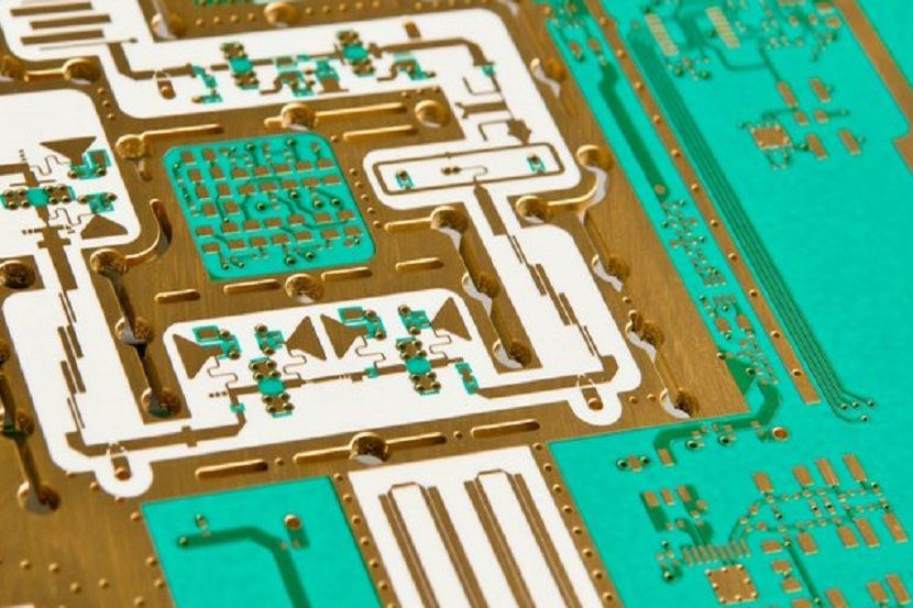
- Layers (2-64)
- HDI: 9+N+9 (Anylayer)
- Low loss pcb material (I-Speed material, FR408HR, Megtron4, EM-888, N4000-13EP, N4000-13, TU-863+, TU-872lk, TU-872SLK, TU-872SLK SP etc)
- High Speed Digital PCB laminate: (I-Tera MT40 / RF, Tachyon-100G, Megtron6/R-5775, TU-883, TU-883SP, IT-968, IT968SE etc)
- RF PCB, Microwave pcb laminate: (RO4450F, RO4350B, RO4835, RO4003, RO4533, Taconic TLY series, TLY-5, RF35, TSM-DS3, Astra MT77, RT/Duroid 5880, RO3203, RO3003 etc)
- Special process PCB: Countersink hole pcb, Press fit pcb, Semi flex pcb, Castellated holes pcb, Cavity pcb etc)
- Special Surface PCB: Selective gold plating pcb, Hard gold pcb, Gold fingers pcb, ENEPIG plating PCB
- Hybrid pcb , Blind and Buried Vias; Filled via capability
- Back drill: Min hole size 15.7mils Depth tolerance +/-6mils
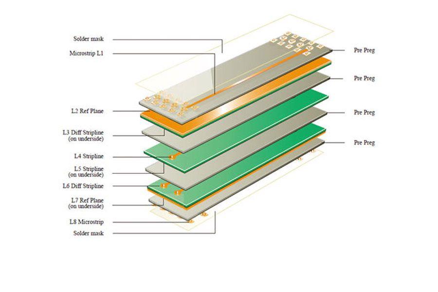
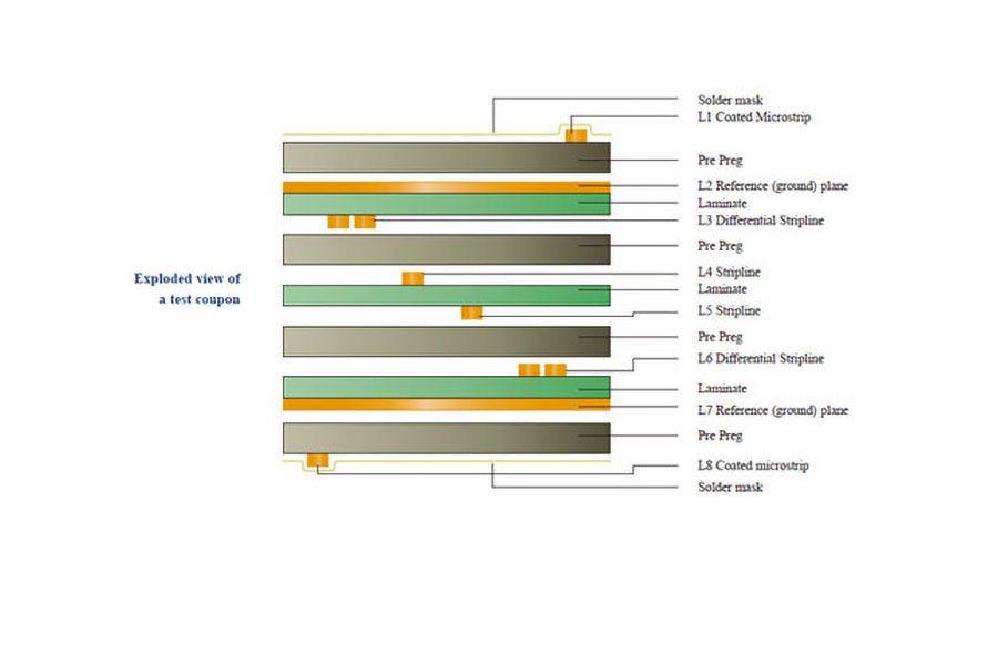
High-speed PCB and RF PCB material comparison
Choosing the right material is an essential part of a high-speed PCB design and fabrication process. PCB materials with the necessary performance characteristics contribute to the optimal performance of high-speed circuit assemblies. Maintaining the signal integrity of high-speed digital signals necessitates the use of PCB material capable of this.
Generally, PCB materials with greater stability (low and stable Dk values at high frequencies and temperatures) will support high-speed boards with low distortion of the higher-order harmonic signal components.
PCB material characteristics such as low loss and dissipation factor (Df) at higher frequencies are key criteria to look for in materials for high-speed digital circuits.
When you’re designing a PCB for a high-speed or RF application PCB, a careful comparison of the electrical and mechanical characteristics of PCB materials can help you select the right base material for your PCB.
These two table provides you with quick access to important information you need for your design.
Our RF PCB Solution
Radio-frequency PCB board materials
RF PCBs are manufactured with certain materials that fulfill high-frequency operation requirements. These materials should have low signal losses, be stable over high-frequency operation, and should be able to absorb high amounts of heat. The dielectric constant (DK), loss tangent (tan δ), and coefficient of thermal expansion (CTE) values also require consistency over wide frequency ranges. Typical values of dielectric constant range from 3 to 3.5 for these boards. Loss tangent values are in the range of 0.0022 to 0.0095 for the frequency range of 10-30GHz.
Apart from all these specific necessities, the material cost and ease of manufacturing are also considered.
Materials that are made of Polytetrafluoroethylene (PTFE), ceramics, and hydrocarbons mixed with one another or with a form of glass are commonly used. Rogers material is a common choice for RF circuit boards. There are different variants of Rogers material available. A few of them are listed below:
- RT/duroid
- RO3000
- RO4000
- Rogers TMM
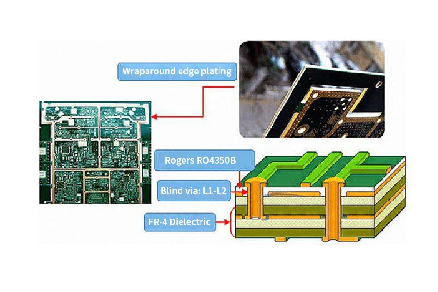
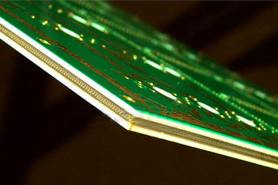
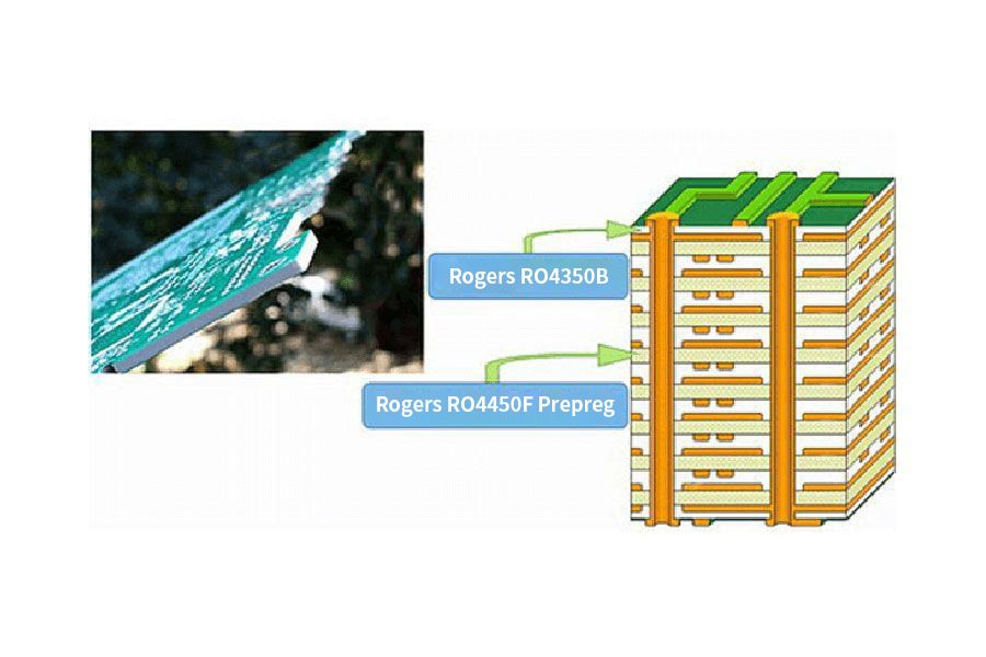
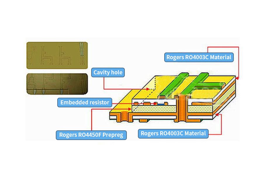
RF PCB
In order to meet increasing demands for Microwave & RF Printed Circuit Boards for our customers all around the world, we have increased our investment over the last few years so that we have become a world-class manufacturer of PCBs using high frequency laminates.
The definition of RF and microwave PCBs is that they contain components that carry RF or microwave signals. These signals vary in frequency from, 50MHz to above 2 GHz, and these frequencies define the differences in components between RF and microwave PCBs and other PCB types.
These applications typically require laminates with specialized electrical, thermal, mechanical, or other performance characteristics that exceed those of traditional standard FR-4 materials. With our many years of experience with PTFE-based microwave laminate, we understand the high reliability and tight tolerance requirements of most applications.
High frequencies require high precision. And extensive expertise. In cooperation with our customers from the automotive and telecommunications industries, we at Hemeixin have developed to become one of the leading manufacturers of printed circuit boards for high-frequency applications in the range from 24 to 77 GHz.
RF PCB design Tips
In order to achieve more reasonable design and better anti-interference ability for high frequency PCB (Microwave RF PCB), design engineer should consider the tips as following:
- Use inner layer as power ground layer, which will have the effect of shielding and even decreasing spurious inductance, shorten length of signal wire, reducing cross interference between signals.
- Circuit layout must be turn with 45 degree angle, which will help to reduce high frequency signal emission and coupling between each other.
- The shorter the better for length of circuit layout.
- The less the better for through holes.
- Layout between layers should be in vertical direction, top layer as horizontal direction and bottom layer as vertical direction, because this will help to reduce the signal interference.
- Increasing copper on ground layer to reduce the signal interference.
- Do package for important signal traces can obviously improve signals anti-interference ability. Of course, we can also do package for interference sources to avoid interference on other signals.
- Signal traces layout should avoid loop, but should layout according to chrysanthemum link.
- In the power section of integrated circuit, bridging decoupling capacitor.
RF PCB Substrate Selection
RF PCBs handle low MHz frequencies to high GHz. The material selection for a PCB is important to ensure signal integrity, reliable operation, and consistency at high frequencies. The factors to consider while selecting PCB material are:
- Dielectric constant
- Thermal expansion coefficient (CTE)
- Loss tangent or dissipation
Some common materials are RO3000, RO4000, RT/Duroid, etc. The copper material selection for an RF PCB stack-up is also essential, as it influences the skin effect on signal propagation.
RF PCB Layer Stacks
Special care needs to be given in RF PCB design stack-ups. Some of the areas to focus on are:
- Isolation between traces
- Distance between components
- Component placement
- Layer arrangement and count
- Power supply decoupling
In RF PCBs, the RF traces are routed on the top layer; the immediate layers are ground and power planes. The immediate ground plane ensures a minimum ground current return path. The non-RF traces are laid on the bottom layer to minimize interference between RF and non-RF components.
RF PCB Trace Design
RF PCB traces are vulnerable to transmission losses and signal interference issues. The main concern in RF trace design is characteristic impedance. The most commonly used RF traces are coplanar waveguides, striplines, and microstrips. Some of the best practices to follow while designing RF PCB traces are:
- To eliminate attenuation, keep the traces as short as possible.
- Never place an RF trace and non-RF trace parallel, as it introduces interference between them.
- Test points should be placed outside the traces to maintain the impedance-matching values of the traces.
- Include curved ends to improve the performance of the RF PCB.
RF PCB design guidelines start with PCB substrate material selection to develop excellent RF PCB boards. Hemeixin can help you design PCB boards that handle RF and non-RF components and devices.
Microwave PCB
RF microwave PCBs are a specialized type of PCBs designed to handle high-frequency signals in the RF and microwave frequency range with minimal signal loss and maximum signal integrity. They are used in a wide range of electronic applications such as wireless communication systems, satellite communication systems, radar systems, and other high-frequency electronic systems. Their design and production require specialized knowledge and experience to ensure the expected performance.
Radio Frequency and Microwave PCBs are a special and innovative type of PCB, designed to operate on signals in the Megahertz to Gigahertz frequency ranges for communication signals in everything from smartphones to military radars. Very specific materials and technology that are not available in many factories are required to build the PCB equipment.
Is PTFE Better Than FR4 PCB Materials with Microwave PCB?
PTFE and FR4 are two of the most used PCB design materials, and it’s important to understand the difference between them. FR4 is a standard defined by National Electrical Manufacturers Association (NEMA), referring to glass-reinforced epoxy laminate material. The "FR" in FR4 stands for "flame retardant." While FR4 materials are common and they cost less, PTFE is a better choice for RF/microwave PCBs operating well above WiFi frequencies. PTFE materials have some important advantages:
- Lower dissipation factor than FR4 materials
- Lower dispersion up to very high frequencies
- Dielectric constant is more stable against temperature changes
- Some laminates can have lower CTE values than FR4
- Materials tend to be available with low-profile copper
One strategy for using PTFE materials alongside standard epoxy resin/fiberglass FR4 materials is to build a hybrid PCB stackup. In this type of design, one or more outer layers can be designed with a low-loss PTFE material to support RF routing. The other layers can then be chosen from standard FR4 materials with higher dielectric constant. This is a useful approach in mixed-signal systems that also have some digital interfaces, but they do not have the low-loss requirements of a typical RF interconnect.
What is a High Frequency PCB?
A high frequency printed circuit board, whether it’s rigid or flex, offers faster signal flow rates and a frequency range of up to 100 GHz. It’s important to note that there are numerous materials designed to operate at high frequency levels. high frequency PCBs are defined by lower dielectric constant (Dk), lower dissipation factor (Df), and low levels of thermal expansion. They are used regularly for HDI technology. They are also used extensively in high speed communications, telecommunications, and RF microwave technology.
The increasing complexity of electronic components and switches continually requires faster signal flow rates, and thus higher transmission frequencies. Because of short pulse rise times in electronic components, it has also become necessary for high frequency (high frequency) technology to view conductor widths as an electronic component.
Depending on various parameters, high frequency signals are reflected on circuit board, meaning that the impedance (dynamic resistance) varies with respect to the sending component. To prevent such capacitive effects, all parameters must be exactly specified, and implemented with the highest level of process control.
Critical for the impedances in high frequency circuit boards are principally the conductor trace geometry, the layer buildup, and the dielectric constant (εr) of the materials used.
Materials Used for High Frequency PCB
Special materials are required to achieve the high frequency provided by this type of PCB. There are a variety of substrate materials that will support your design and may differ based on signal speeds required and the application/environment of the circuit board.
In terms of price, FR4 is the least expensive compared to dedicated high speed materials and Teflon, with Teflon being the most expensive. Though, FR-4 starts to drop off in performance when signal speed edges above 1.6ghz
Newer generation substrates, Teflon, and flex circuits are the best options when it comes to Dk, Df, water absorption, and survivability in the environment
If a printed circuit board requires a frequency above 10GHz, newer generation substrates, Teflon, and Flex substrates are your best option since they are far superior to traditional FR-4 material.
The most common suppliers of high speed substrates are Rogers, Isola, Taconic, Dupont, and Megtron materials by Panasonic. All of these materials typically are lower Dk and lower loss.
High Frequency PCB Applications
High frequency rigid and flex PCBs are used in many products and across many industries, including:
- Cell phone
- Telecommunications
- Military and aerospace
- RF microwave
- Automotive (mainly LIDAR, which is a mini radar that communicates a vehicle’s surroundings)
- High-density interconnect and high-speed design applications
For many applications, it is sufficient to use FR4 material with an appropriate layer buildup. In addition, we process high-frequency materials with improved dielectric properties. These have a very low loss factor, a low dielectric constant, and are primarily temperature and frequency independent.
Additional favourable properties are high glass transition temperature, an excellent thermal durability, and very low hydrophilic rate.
We use (among others) Rogers or PTFE materials (for example, Teflon from DuPont) for impedance controlled high frequency circuit boards. Sandwich buildups for material combinations are also possible.
High Frequency PCB Design
Hemeixin supports you starting immediately in the design phase. We help you to find appropriate substrates, dimensioning the conductor width and spacing, as well as with calculating the impedances.
Our offer for high frequency circuit boards:
- High frequency-material (low-loss), e.g. PTFE substrate
- Impedance controlled multilayers
- Sandwich buildup / hybrid layer buildup for material combinations
- Microvias strating from 75µm
- Controlled production line / with comprehensive test certificate, as needed
- Backdrill
What materials are used for high-frequency PCBs?
When it comes to the cost of FR4, PPO, and Teflon laminates, FR4 is the least expensive, while Teflon is the most costly. Teflon is the best in terms of DK, DF, water absorption, and frequency characteristics. Only Teflon PCB substrate can be used to produce products that require frequencies more than 10GHz. Teflon’s performance is significantly superior to that of other substrates, yet, Teflon has the disadvantage of great heat resistance.
PTFE or polytetrafluoroethylene is a synthetic thermoplastic fluoropolymer and is the second most commonly used PCB laminate material. It offers consistent dielectric properties at a higher coefficient expansion than standard FR4. These two laminates, FR4 and PTFE, quickly became the 2 options for all PCBs coming to market.
The PTFE is commonly used in a higher-speed, higher-frequency technology. One example is microwave technology: the PTFE has a higher coefficient of thermal expansion (CTE). This makes it a good choice where the PCB could see changes in temperature.
The base PTFE had its challenges to overcome with the addition of woven glass assisted in the stability or size changes of the laminate due to fluctuating temperature. Later, ceramic fillers and microfiber glass were introduced to increase the dielectric constant (Dk) values. PTFE with additives such as glass or ceramic improved and stabilize the DK, allowing for a better signal between parts to be had.
The additional cost for this type of material is significant from FR4. It is more costly to produce and typically the quantity of PCBs is smaller for the purchase. This, compiled with the part’s physical size, is also typically smaller in the X,Y, driving up the cost to manufacture.
The supplier imposes a MOQ on laminate purchase to multiple sheets, leaving stock on the shelf for an undetermined amount of time. This cost is passed on to the consumer in the piece price or laminate cost so as to encourage consumption and ease the pain of purchasing and having stock for long periods of time. Introducing multiple parts on one panel has become more common to aid the customer in keeping costs down; we have seen 8 or 12 different PCBs on a single array for a one-time buy versus buying 5 pieces of 8 or 12 different parts in a single purchase each. This saves the customer on NRE passing as 1 instead of 8 or 12, but it also assists production on the consumption of panels where the physical size is small, so it is allowed.
When Do You Need an RF PCB Material?
This is a fair question and it relates to some important tasks in systems analysis. There are a few different considerations a designer should examine when qualifying an alternative PCB substrate material should be used. Here’s a short list of some dimensions you might look at when selecting an RF PCB substrate material.
- Loss tangent: This is the first major area that PCB designers will use to start comparing material options.
- Dielectric constant: Although this is sometimes misunderstood, and everyone tends to just go for low-Dk laminates, but high-Dk laminates can also have low loss tangent and other benefits.
- Thermal properties: There are multiple thermal properties, but the most important are probably glass transition temperature and CTE.
- Workability in fabrication: Designers leave this up to their fabricator at their own peril. It’s best to contact your fabricator regarding availability of materials, their ability to work the board, and availability of materials.
- Thickness: You can’t just choose any thickness you want, you’ll need to check with your fabricator on their preferred stackup. If you know which layer thicknesses they can support, you can usually get your design close enough to the fabricator’s specifications.
- Dispersion: I’ve put this at the bottom of the list as it tends to matter least for mmWave applications. The bandwidths in mmWave devices may be small enough that dispersion is negligible, but you should still check on this where possible.
Many years of experience in processing special high-frequency materials have made us the perfect partner for you and your RF PCB project.
We use special materials for achieving the high frequency operations of our HF PCBs. Depending on the range of signal speeds of the application, we use a variety of substrate materials that are the best suitable.
Ceramic-filled PTFE composites, which have exceptional electrical and mechanical stability. Rogers RO3000 series circuit materials have consistent mechanical properties, regardless of the dielectric constant (Dk) selected, which allows multi-layer board designs that use different dielectric constant materials without encountering war-page or reliability problems. The Taconic RF series of products has a low dissipation factor with high thermal conductivity possible so it will not oxidize, yellow, or show upward drift in dielectric constant and dissipation factor like its hydrocarbon-based competitors.
Ultra-low Loss, Highly Heat-Resistant, Halogen Free Megtron 6 circuit board material. With high glass transition temperature (Tg) and the low expansion ratio of hydrocarbon resin-based MEGTRON 6 - makes it ideal for High-Density Interconnect (HDI) and high speed (above 3 GHz) constructions.
Woven Glass Reinforced PTFE laminates are manufactured with very lightweight woven fiberglass and are more dimensionally stable than chopped fiber reinforced PTFE composites. Materials such as the Taconic TL family of products have a low dissipation factor, and this is perfect for radar applications designed at 77 GHz as well as other antennas in millimeter-wave frequencies.
Hydrocarbon ceramic laminates are used in microwave and millimeter-wave frequency designs as this low loss material offers easier use in circuit fabrication and streamlined properties over traditional PTFE materials. Rogers RO4000 series of products come in a wide range of DK values (2.55-6.15) and have above average thermal conductivity (.6-.8).
Filled PTFE (random glass or ceramic) composite laminates such as the Rogers RT/duroid® high frequency circuit materials have low electrical loss, low moisture absorption, and low outgassing properties that are preferred in space applications.
Thermoset microwave laminates combine low thermal coefficient of dielectric constant (Dk), a copper matched coefficient of thermal expansion and excellent mechanical reliability. Rogers TMM materials are high-frequency laminates ideal for high-reliability strip-line and micro-strip applications.
Benefits Of RF PCB
RF PCB boards come with a wide variety of benefits for MHz and GHz applications:
- It allows High Frequency signals to travel fast with less impedance.
- Since it is possible to have multilayer board stack-up, is makes for both, optimal performance and reduced costs.
- They lend themselves to seamless usage in high temperatures. For applications that have to work in high environmental temperatures, therefore, their importance cannot be overstated.
- It is easy to place fine pitch components, which is increasingly becoming the need of the hour.
RF PCB Board Applications
RF boards have a multitude of different applications, including wireless technologies, smart phones, sensors, robotics and security. With the advent of new technologies that are pushing the limits of electronics, the demand for RF boards is on the rise.
Finding a capable RF PCB manufacturer is critical to make sure the boards are fabricated to high quality standards and on-time. Our reputation speaks for itself. We pride ourselves on bringing the most demanding layout concepts to reality.
RF PCB Manufacturer
As high frequency PCB manufacturer, Hemeixin makes both rigid and flexible types of boards. Our high frequency PCBs offer faster signal flow for frequencies up to 100 GHz. Although numerous materials are available for high frequency operation, Hemeixin uses materials for HF PCBs that exhibit a few common features like low dielectric constant or Dk, low dissipation factor or Df, and low coefficient of thermal expansion or CTE. We use the materials for high frequency PCBs also for our boards using HDI technology. Industries using our high frequency PCBs include RF microwave, telecommunications, high speed communications, and more.
Benefits of Rogers PCB
- They are well suited for harsh environmental conditions.
- Rogers PCB show significantly less moisture absorption as well as improved thermal management.
- RO4000 material’s thermal co-efficient of expansion is akin to that of copper that offers dimensional stability.
- They are also known to display better impedance control.
- They are extremely cost-effective when it comes to circuit fabrication.
- They are known for lower di-electric loss, lower signal loss, as well as low cross-over.
What is Rogers PCB
RO4000 hydrocarbon ceramic laminates are designed to offer superior high frequency performance and low cost circuit fabrication. The result is a low loss material which can be fabricated using standard epoxy/glass (FR-4) processes offered at competitive prices.
The selection of laminates typically available to designers is signifi cantly reduced once operational frequencies increase to 500 MHz and above. RO4000 material possesses the properties needed by designers of RF microwave circuits and matching networks and controlled impedance transmission lines. Low dielectric loss allows RO4000 series material to be used in many applications where higher operating frequencies limit the use of conventional circuit board laminates. The temperature coeffi cient of dielectric constant is among the lowest of any circuit board material , and the dielectric constant is stable over a broad frequency range . For reduced insertion loss, LoPro® foil is available. This makes it an ideal substrate for broadband applications.
RO4000 material’s thermal coeffi cient of expansion (CTE) provides several key benefi ts to the circuit designer. The expansion coeffi cient of RO4000 material is similar to that of copper which allows the material to exhibit excellent dimensional stability, a property needed for mixed dielectric multi-layer boards constructions. The low Z-axis CTE of RO4000 laminates provides reliable plated through-hole quality, even in severe thermal shock applications. RO4000 series material has a Tg of >280°C (536°F) so its expansion characteristics remain stable over the entire range of circuit processing temperatures.
RO4000 series laminates can easily be fabricated into printed circuit boards using standard FR-4 circuit board processing techniques. Unlike PTFE based high performance materials, RO4000 series laminates do not require specialized via preparation processes such as sodium etch. This material is a rigid, thermoset laminate that is capable of being processed by automated handling systems and scrubbing equipment used for copper surface preparation.
RO4003C™ laminates are currently offered in various confi gurations utilizing both 1080 and 1674 glass fabric styles, with all confi gurations meeting the same laminate electrical performance specifi cation. Specifi cally designed as a drop-in replacement for the RO4003C™ material, RO4350B™ laminates utilize RoHS compliant fl ame-retardant technology for applications requiring UL 94V-0 certifi cation. These materials conform to the requirements of IPC- 4103.
Why Rogers PCB material?
Although Rogers laminates are a bit more expensive than other materials, they perform well in challenging conditions. Here are the reasons to go for Rogers materials:
- Reduced electrical signal and dielectric losses
- Low outgassing when used in space applications
- Improved controlled impedance
- Most suitable in high power applications
- Enhanced plated through hole (PTH) reliability
- Improves heat sink performances
- Better dimensional stability
- Low CTE values make it ideal for space and radar applications
- Offers a wide range of dielectric constants (2.55 to 10)
What is RO4350B PCB
RO4350B laminates provide tight control on dielectric constant (Dk) and maintain low loss while utilizing the same processing method as standard epoxy/glass. Available at a fraction of the cost of conventional microwave laminates, RO4350B laminates do not require the special through-hole treatments or handling procedures as PTFE based materials. These materials are UL 94 V-0 rated for active devices and high power RF designs.
Rogers RO4350B PCB including:
A glass-fi ber reinforced hydrocarbon ceramic laminate is used to manufacture the Rogers 4350B. You can fabricate Rogers 4350B boards using conventional FR-4 processing methods. Some of the signifi cant features of Rogers 4350B are:
- Excellent dimensional stability: The CTE of this material is almost equal to that of copper. This enables the board to be dimensionally stable even at extreme temperatures.
- Constant Dk at various frequencies: Stable Dk makes them suitable for controlled impedance boards.
- Low insertion and dielectric losses: Rogers 4350 laminates incorporate low-profile copper which in turn reduces the signal losses. This property makes them the right choice for broadband and other high-speed applications.
- CAF resistant: Avoids formation of conductive filaments for high-voltage applications.
- Superior thermal resistance: Lower CTE along the Z axis and higher Tg (280°C) enable them to operate in a desired at higher temperatures
Features of rogers 4350b material:
- Dk of 3.48 +/- 0.05
- Dissipation factor of 0.0037 at 10 GHz
- Low Z-axis coefficient of thermal expansion at 32 ppm/°C
- Processes like FR-4 at lower fabrication cost
- Competitively priced
- Excellent dimensional stability
What is RO4003C PCB
Offered in various configurations, RO4003C laminates utilize both 1080 and 1674 glass fabric styles with all configurations meeting the same laminate electrical performance specification. RO4003C laminates provide tight control on dielectric constant (Dk) and low loss while utilizing the same processing method as standard epoxy/glass but at a fraction of the cost of conventional microwave laminates. Unlike PTFE based microwave materials, no special through-hole treatments or handling procedures are required.
RO4003C materials are non-brominated and are not UL 94 V-0 rated. For applications or designs requiring a UL 94 V-0 flame rating, RO4835™ and RO4350B™ laminates do meet this requirement.
Rogers RO4003C PCB including:
- Dk of 3.38 +/- 0.05
- Dissipation factor of 0.0027 at 10 GHz
- Low Z-axis coefficient of thermal expansion at 46 ppm/°C
- Ideal for multi-layer board (MLB) constructions
- Processes like FR-4 at lower fabrication cost
- Designed for performance sensitive, high volume applications
- Competitively priced
Rogers PCB manufacturing Tips
Surface preparation
- A chemical process consisting of cleaning, micro-etching, water rinsing, and drying is the preferred method of surface preparation,especially for thinner core materials.
- Mechanical scrubbing should only be considered for the cores that are thicker than 60 mils. Scrubbing should also be performed with reduced pressure to avoid imparting scratches on the laminates since scratches lessen the spacing between traces.
Multi-layer bonding
- Rogers cores can be prepared for multi-layer bonding using any oxideor oxide alternative process that is also used for high Tg FR4 material systems.
- Inner-layer cores should be baked in a rack for 30 minutes at 107°C to 121°C (225F to 250F) prior to layup.
Drilling
- Drilling vias/holes using CO2, UV or CO2/UV combination lasers are preferred when aspect ratios permit.
- A post-laser clean with alkaline permanganate or CF4/O2 plasma can be used to ensure a good electrical connection to copper pads at the base of vias.
- Standard aluminum or pressed phenolic entry and exit materials are acceptable for mechanical drilling.
Copper plating and outer-layer processing
- Panel and pattern processing using electrolytic tin plating and acid copper is compatible with Rogers.
- The materials can then be treated using any standard strip/etch/strip(SES) method after plating.
- After etching, surfaces should bond very well to direct screened and photo-imageable solder masks.
- A short bake for 30-60 minutes at 110°C to 125°C may be required to ensure the board surfaces are dry prior to applying the solder mask .
With the advancements in electronic devices, circuit board materials such as Rogers are a must to ensure minimum signal losses in high-frequency applications such as aerospace, defense, and communication systems.
Rogers PCB Manufacturer
The use of high frequency rogers printed circuit board material is imperative when it comes to creating PCBs for critical applications that particularly need low signal loss as well as low dielectric loss. Such material is also the need of the hour when signal integrity and impedance matching are of utmost importance.
At Hemeixinpcb, we provide Rogers printed circuit boards, one of the well-known names, when it comes to Rogers PCB manufacturing:
- Dielectrics
- Laminates
- Prepregs
Their high-quality materials, are especially known for their ability to withstand harsh environmental conditions.
As a Rogers PCB Manufacturer, we are fully equipped to manufacture eponymous printed circuit boards created from material sourced from Rogers that is known for their durability and reliability. We provide high mix printed circuit boards, high frequency rogers PCB, RF rogers printed circuit boards, SMT rogers circuit boards, Rogers PCB prototype and more. The range of manufacturing printed circuit boards are reliable, efficient and high performance for any type of specialty applications.
- PCB Technology
- PCB Material
- Epoxy Filled Vias
- Heavy copper circuit board
- HDI Micro vias PCB
- Controlled Impedance
- RF & Microwave PCB
- Rigid-Flex Circuit
- Bending And Folding
- Thermally Conductive PCB
- Flex PCB design guidelines
- Rigid flex PCB design guidelines
- HDI PCB design guidelines
- Heavy copper PCB design guidelines
- Flexible PCB design issues
- Flex-Rigid PCB design issues
- Turn-key PCB Assembly design issues
- PCB Trace Width Calculator
-
Phone:
-
Email:This email address is being protected from spambots. You need JavaScript enabled to view it.


