-
![High Frequency Low Loss PCB manufacturer]()
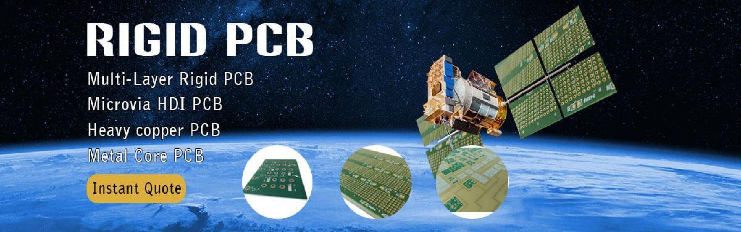
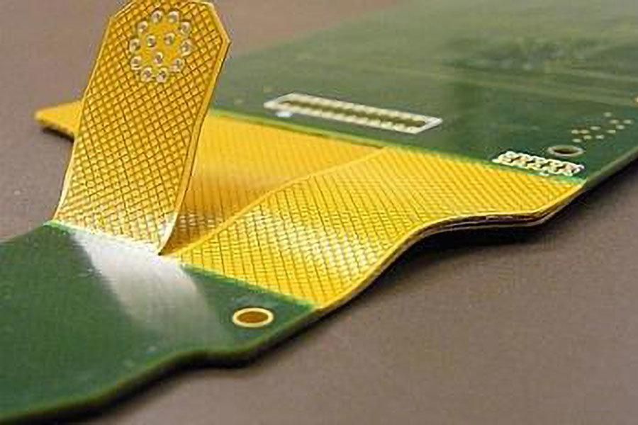
HDI Blind and Buried Microvias PCB manufacturing with High Frequency Low Loss PCB Material, Rigid flex pcb and Flexible circuit
-
![flex circuit manufacturer]()
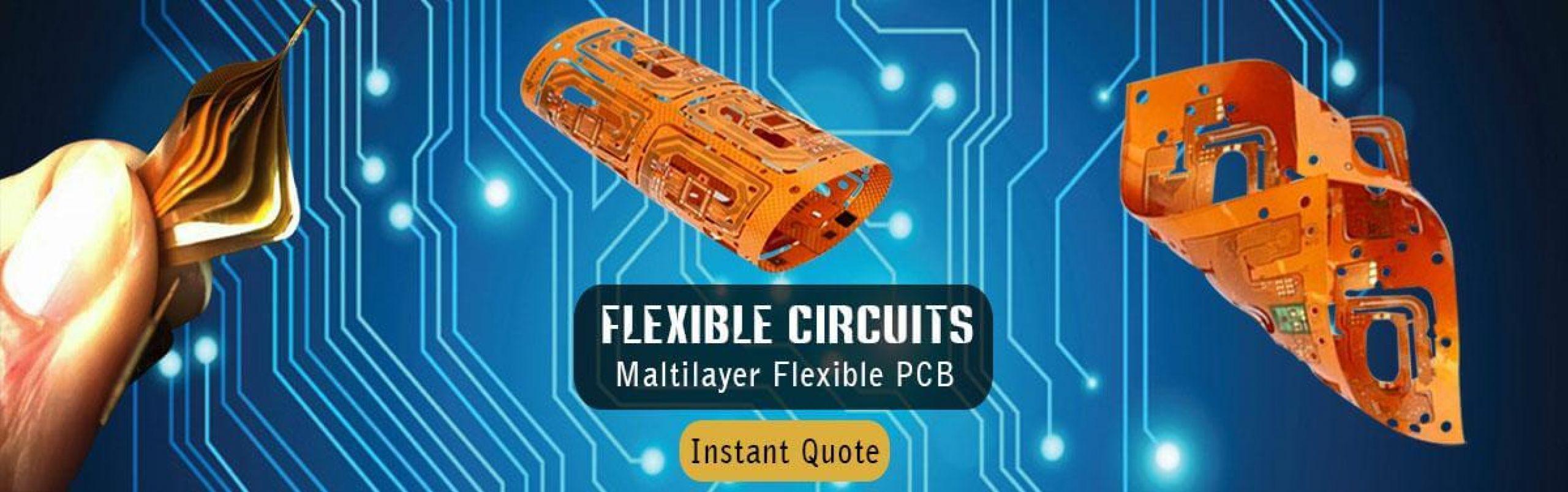
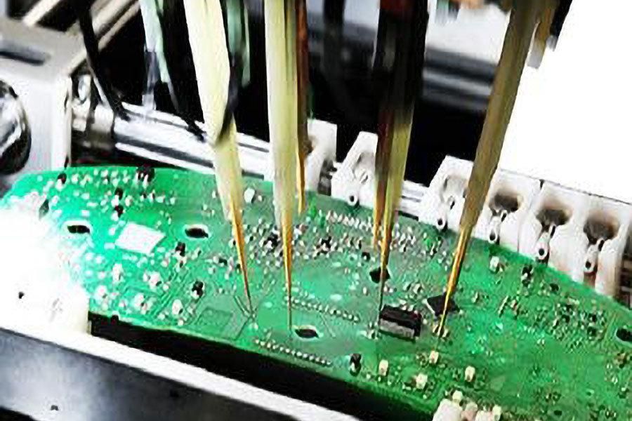
HDI Blind and Buried Microvias PCB manufacturing with High Frequency Low Loss PCB Material, Rigid flex pcb and Flexible circuit
-
![rigid flex circuit manufacturer]()
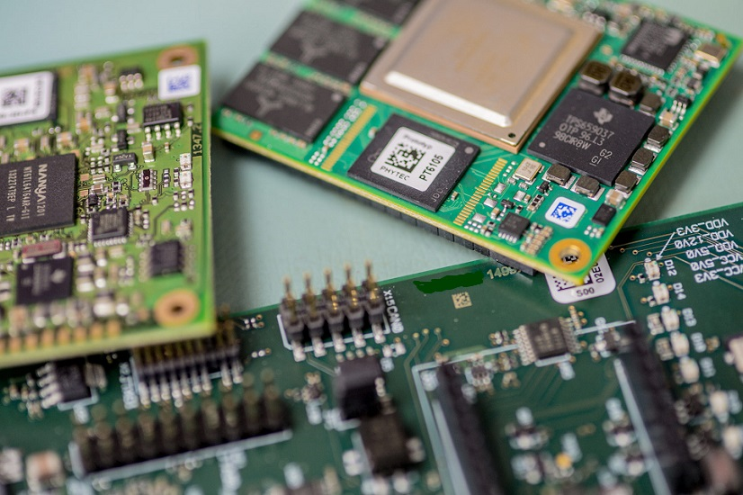
HDI Blind and Buried Microvias PCB manufacturing with High Frequency Low Loss PCB Material, Rigid flex pcb and Flexible circuit
-
![Turnkey pcb assembly manufacturer]()
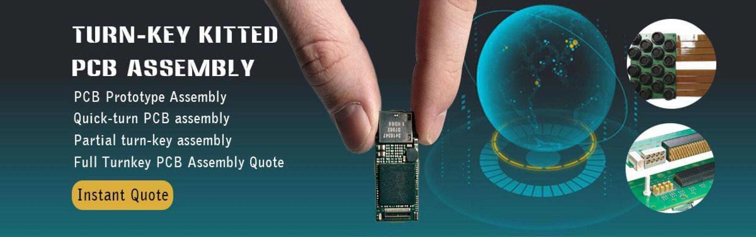
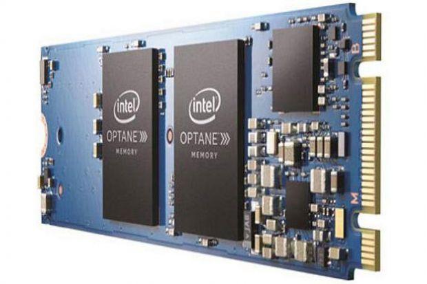
HDI Blind and Buried Microvias PCB manufacturing with High Frequency Low Loss PCB Material, Rigid flex pcb and Flexible circuit
-
![RF pcb manufacturer]()
HDI Blind and Buried Microvias PCB manufacturing with High Frequency Low Loss PCB Material, Rigid flex pcb and Flexible circuit


LeiterplattenHerstellung: HDI Leiterplatten & RF Leiterplatten
Als ein führender Leiterplattenhersteller bietet HemeixinLeiterplatten ein komplettes Sortiment an starren Leiterplatten von ein- und doppelseitig aufwärts an, unterstützt aber auch lasergebohrte Mikrovias, HohlraumLeiterplatten, schweres Kupfer bis zu 30 Unzen, Via-in-Pad, Mikrowellen- und RF-Leiterplatten mit bis zu 58 Lagen und andere.
- Lagenzahl: 2~58L
- HDI-Leiterplatte, Hochfrequenz-Leiterplatte
- Blind- und verdeckte Durchführungen (mechanisches und Laserbohren)
- Mit Epoxidharz gefüllte und mit Kupfer verschlossene Mikrolöcher
- Polyimid-Laminat für starre Leiterplatten (Alron85N, Isola P95, Isola P96, Ventec VT901 usw.)
- Verlustarmes Leiterplattenmaterial (I-Speed-Material, FR408HR, Megtron4, EM-888, N4000-13EP, N4000-13, TU-863+, TU-872lk, TU-872SLK, TU-872SLK SP usw.)
- Digitales Hochgeschwindigkeits-Leiterplattenlaminat: (I-Tera MT40 / RF, Tachyon-100G, Megtron6/R-5775, TU-883, TU-883SP, IT-968, IT968SE usw.)
- RF-Leiterplatten, Mikrowellen-Laminat: (RO4450F, RO4350B, RO4835, RO4003, RO4533, Taconic TLY-Serie, TLY-5, RF35, TSM-DS3, Astra MT77, RT/Duroid 5880, RO3203, RO3003 usw.)
- BGA Pitch bis zu : 0,15mm (min)
- Min. Leiterbahnbreite/Abstand: 0.002"/0.002"
- Gestaffelte, gestapelte und übersprungene Mikrovias HDI: 9+N+9 (beliebige Schicht hdi)
- Rückwärts bohren: Min Lochgröße 15.7mils Tiefe Toleranz +/-6mils
- Cavity Leiterplatten Prozess
Starrflex-Leiterplatten & Flex Leiterplatten
HemeixinLeiterplatten kann die Produktion von starr-flexiblen und flexiblen Leiterplatten und HDIs für hochzuverlässige Anwendungen anbieten, mit Merkmalen bis zu 25 µm und einem flexiblen dielektrischen Kern bis zu 25 µm. Mit der Revolution bei tragbaren Kommunikationsprodukten im letzten Jahrzehnt sind starrflexible Schaltungen zu einer bevorzugten Designlösung für komplexe, dreidimensionale Produktmontage und fortschrittliche Anforderungen an die Oberflächenmontage von Komponenten geworden.
- Doppelseitiger/einseitiger Flex
- Multilayerr Flex
- Mehrschichtig flexibel starr
- Gemischte dielektrische (hybride) Konstruktionen
- Schnelles Drehen Starrer Flex
- HDI Micro-Vias - Blind, Buried, Staggered und Stacked Vias
- Mit Epoxidharz gefüllte und mit Kupfer verschlossene Mikrolöcher
- Sequentieller Aufbau
- Hohe Geschwindigkeitsanforderungen
- Großformatige Schaltung
Leiterplattenbestückung
HemeixinLeiterplatten ist ein One-Stop-Shop für alle Ihre Bedürfnisse im Bereich der Leiterplattenbestückung. Wir bieten Inhouse-LeiterplattenFertigung, Montage und schlüsselfertige Dienstleistungen innerhalb von fünf Tagen oder weniger.
Wir sind auf die schnelle Fertigung von Prototypenenn und Kleinserien spezialisiert. Für die Produktion von zuverlässig bestückten Leiterplatten verwenden wir modernste Anlagen.
- Kostenvoranschlag für elektronische Bauteile online
- Online-Kostenvoranschlag für Flex-, Starrflex- und starre Leiterplatten
- Leiterplatten Bestückung Kosten Online-Angebot
- Flex-, Starrflex- und starre Leiterplattenbestückung
- SMD, Durchstecktechnik und gemischte Technologie
- Tafelgrößen bis zu 20" x 24"
- Komplexe, hochdichte Baugruppen
- PBGA, CBGA, TBGA, FPGA, CGA, LGA
- Paket auf Paket (PoP) Montage
- Mikro-BGA (0,4 mm)
- 0402s, 0201s, 01005s
- Wellen- und Selektivlöten
Express Leiterplatten & Leiterplatten Prototypen
Wir wissen, wie wichtig es ist, dass die von Ihnen bestellten Leiterplatten so schnell wie möglich zur Montage gelangen. Deshalb haben wir alles daran gesetzt, unsere Kernkompetenzen zu stärken und unsere LeiterplattenProduktionskapazitäten zu verfeinern, um sicherzustellen, dass wir Ihren Auftragstermin in kürzester Zeit einhalten können.
Wir wissen nicht nur, wie wichtig eine schnelle Abwicklung für den Erfolg Ihres Projekts ist, sondern auch, dass die daraus resultierende Qualität ebenso wichtig ist. Mit unserer integrierten Inhouse-Anlage, 687 Mitarbeitern, 87+ engagierten Ingenieuren, 42 verschiedenen LeiterplattenFertigungsstationen und einem 24/5 Produktionsplan können wir alle Leiterplatten Prototypenenn-Bestückungsprojekte mit knappen Fristen schneller erfüllen als die durchschnittlichen Durchlaufzeiten, die die meisten LeiterplattenDienstleister erreichen können - und das natürlich mit Qualität. Das bedeutet kürzeste Durchlaufzeiten und höchste Qualität auch für jedes HDI-Projekt.
- Quick Turn PCB-Fertigung
- PCB für hohe Temperaturen
- Hochfrequenz-Leiterplatte
- Flexible Leiterplatte
- Starrflex-Leiterplatte
- Rogers PCB
- PTFE PCB
- Metallkern-Leiterplatte
- RF-Leiterplatte
- Hochgeschwindigkeits-Signal-Leiterplatte
- Schweres Kupfer PCB
- Hybrid-Leiterplatte
- ATE-LEITERPLATTE
- BGA-Bestückung
- Prototypische PCB-Montage
- Quick Turn PCB Montage
- Konsignierte PCB-Baugruppe
- Komplette schlüsselfertige PCB-Montage
Leiterplatten Prototypen service
| Layers | Standard Delivery | Fast Delivery | Express Delivery |
|---|---|---|---|
| 2 | 5 days | 3 days | 1 day |
| 4 | 6 days | 4 days | 2 days |
| 6 | 7 days | 5 days | 3 days |
| 8 | 8 days | 6 days | 3 days |
| 10 | 10 days | 7 days | 4 days |
| 12 | 12 days | 7 days | 5 days |
| 14 | 12 days | 8 days | 5 days |
| 16 | 13 days | 8 days | 5 days |
| 18 | 14 days | 10 days | 6 days |
| 20 | 15 days | 10 days | 6 days |
Since China’s New Year is approaching, we'd like to inform you that we'll have 5-day holiday from Jan. 21st to Jan. 25th (GMT+8) during which your question or email may not be replied immediately. However, Microvia HDI PCB, RF PCB, Rigid-Flex PCB, Flex PCB quotation or orders can be submitted online or email to us as usual.
In order not to get your manufacturing efficiency reduced, we strongly suggest you submit quotation or order in advance so that manufacturing can be done or started at least before our public holiday. Thank you for your understanding and patience.
Our PCB factory workers start holiday earlier (13th Jan). For bare PCB orders, please kindly calculate the lead date before you place the order. Some boards cannot be finished before our holiday and will be delayed to February.
Together we can plan the best solution for your needs!
Our teams are well prepared to help you put your requests into action and answer any questions you may have.
Do not hesitate to contact Hemeixin for further information about lead time and recommendations for your order planning.
Contact: Diese E-Mail-Adresse ist vor Spambots geschützt! Zur Anzeige muss JavaScript eingeschaltet sein!
Send us your PCB, Rigid flex PCB, flexible circuit data files and we will run a complete DFM check for manufacturability. Experience how our engineering support gives customers the most in-depth feedback, with exact accuracy, eliminating delays and quality problems discovered before fabrication. We will check below items carefully.
- Drill Checks
- Solder Mask Checks
- Silkscreen Checks
- Controlled Impedance Checks
- Stackup Checks
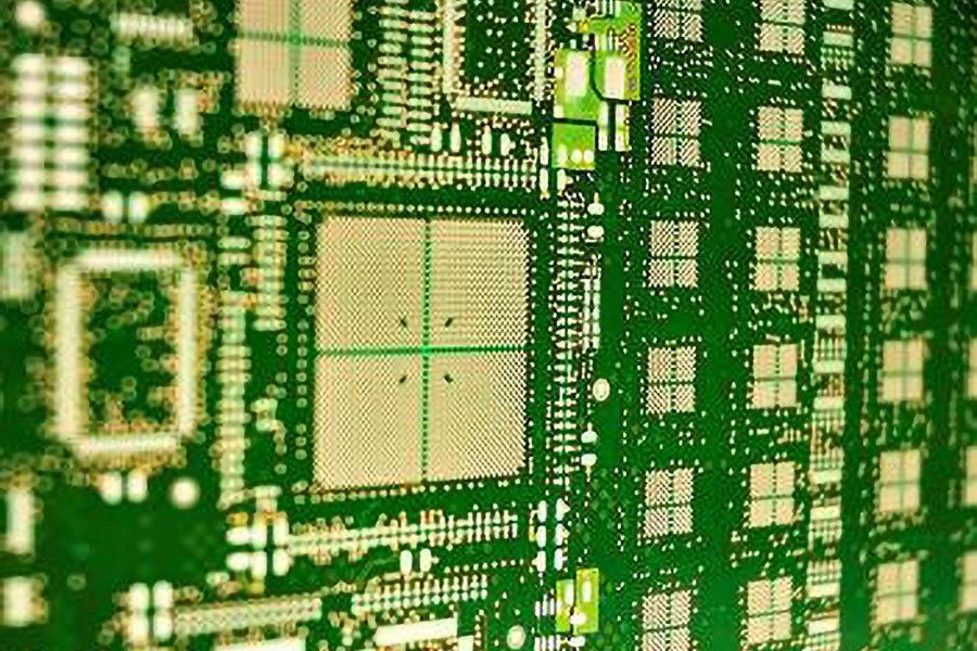
- HDI PCB via holes Structures
At some level of circuit complexity, turning to an architecture with blind and buried vias will result in better yield and lower cost than would a through-hole design. Learn more from How to BGA Fanout Routing in your HDI PCB and HDI PCB design guidelines
Sometimes, you can’t fit all your connections on one layer. This is where vias come to your rescue!
Vias are barrel shaped vertical conductive holes that make connections between multiple layers of a PCB. The IPC defines eight different types of vias, but we’re going to talk about blind and buried vias; the two you’re most likely to work with.
A blind via connects an outer layer of the board to inner layers and doesn’t go through the entire board. A buried via connects inner layers without reaching the outer layers. And a through hole via goes all the way through, from top to bottom, connecting all layers.

Fitting More on Smaller Boards
Blind and buried vias provide electrical connections from the outer layers to the inner layers as well as in between the inner layers, and are used when you have limited space on your PCB. Buried vias are hidden beneath the layers and free up surface space without impacting the traces or surface components on the top or bottom layers. Blind vias also free up space, can be essential for fine pitch BGA components and have the added benefit of helping reduce signal stubs through the drilling process as the via terminates at the last connected layer.
You mostly see blind and buried vias in High density interconnect (HDI) PCBs. HDIs provide benefits such as increased layer density, improved power delivery and use of much smaller pitch devices. The hidden vias help keep the board light and compact. It is common to see blind and buried vias in electronic products like, cell phones, laptops, and medical devices to name a few.
Incorporating blind vias and buried vias make more connections and higher board density possible. But not without drawback. Vias add extra steps to manufacturing and testing, which come with added costs.


