HDI PCB design guidelines
High-Density Interconnection (HDI) PCB design guidelines
Printed Circuit Board (PCB) manufacturers typically follow three types of stackups for boards they will assemble with high-density packages:
-
Standard Lamination with Vias or Plated Through Holes
-
Sequential Lamination with Plated through, Blind, and Buried Vias
-
Lamination Buildup with micro vias
Among the three above, the last is especially suitable for High Density Interconnect PCB (HDI PCB). Hemeixin Electronics Co.,Ltd., eminent HDI PCB manufacturer,recommends using lamination buildup with microvias for HDI printed circuit boards that have high pin-count Ball Grid Arrays (BGA) and other fine-pitch packages, as each type has its own advantages and disadvantages.
For instance, standard lamination with through vias may be low cost for 28 layers and below, but is very difficult to route when multiple BGAs with over 1500 pins and less than 0.8 mm pitch are involved. Likewise, sequential lamination with blind and buried vias have potentially shorter via stubs and fairly simple via models, with smaller via diameters than those required for through hole vias. Costing more than the standard lamination with through vias, sequentially laminated boards maintain the same minimum trace widths and their practical reliability limits their number of layers to a maximum of two or three.
Above limitations and more are leading to a larger number of HDI PCB manufacturers moving towards building up laminations with microvias and other advanced features for HDI PCBs. Advantages of the microvia HDI PCB design include achieving very high route density with fewer layers, as the traces and vias have much smaller dimensions comparatively. In microvia HDI PCBs, the potential for a lower number of layers comes from the effective use of patterns with microvias, as this opens up more space for routing, providing the only applicable way of designing with several large, fine-pitch BGAs with pitch measuring 0.8 mm or lower.
Offering the lowest cost for high frequency, high-density boards, HDI technology, with suitable stackup definition, also improves power and signal integrity in high frequency PCBs. Although typical materials fabricators use for HDI PCBs do well in processes requiring RoHS, use of newer materials has the potential of higher performance with the lowest costs. Notably, these newer materials are not suitable for fabrication of boards using standard or sequential lamination.
HDI is one of the more complex pcb board fabrication processes we specialize in. We use SBU technology, which allows sequential addition of more pairs of layers to form a multilayer core, to create this type of highly integrated PCB.
SBU pcb is a multilayer technology that can be achieved by putting a dielectric element and a copper foil on both top and bottom of the core before it is submitted to laser drilling, image transferring, and etching processes. Multilayer PCBs designed through this technological procedure are marked by a sequence of numbers and Ns, (e.g., 1+N+1, 2+N+2, etc.), where N represents the number of layers that form the core and the numerical values represent the number of layers added.
To provide modern PCB designers with a review of robust rules and methods that will allow them to design a highly reliable printed circuit board with the lowest cost, most commonly used features, and least number of manufacturing issues (that may result in a no-bid, engineering questions, placing the job on hold, or negatively impact the final yield).
High Density Interconnect (HDI) circuit board designs have a higher wiring and pad density than conventional PCBs, along with smaller trace widths and spaces. They require advanced PCB technologies such as blind vias, buried vias, and microvias. HDI PCBs are usually more costly than conventional PCBs due to the complex build-up process involved in fabrication.
Here we only wish to provide the minimums that if adhered to will provide the designer with a highly reliable physical PCB.
Below guildelines including these contents for Blind Vias, Buried Vias & Microvias pcb;
- Footprint Design Assistance
- HDI Microvia Standard Design Rules
- HDI Microvia Types definition
- Cost of MicroVia HDI pcb Types
- Plated Through High Aspect Ratio
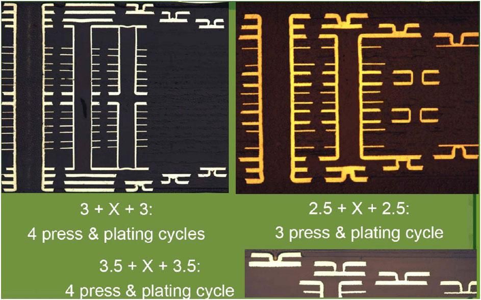
- lamination cycles up to 6 times for Stacked Microvia
Footprint Design Assistance

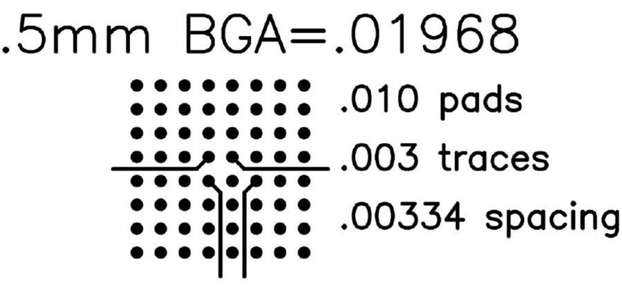
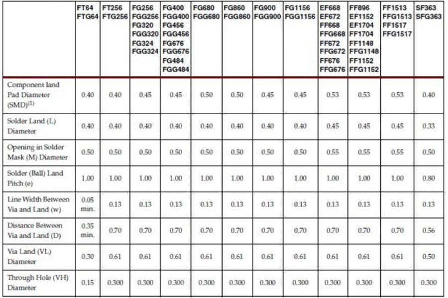
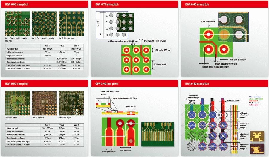
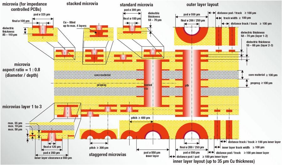
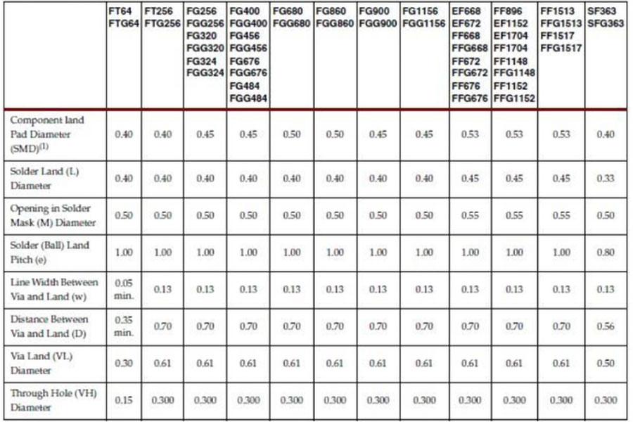
HDI Microvia PCB Standard Design Rules
HDI pcb types definition;
- 1 + n + 1 HDI pcb 1 layer for laser microvias, n layers for inner layers between the microvias.
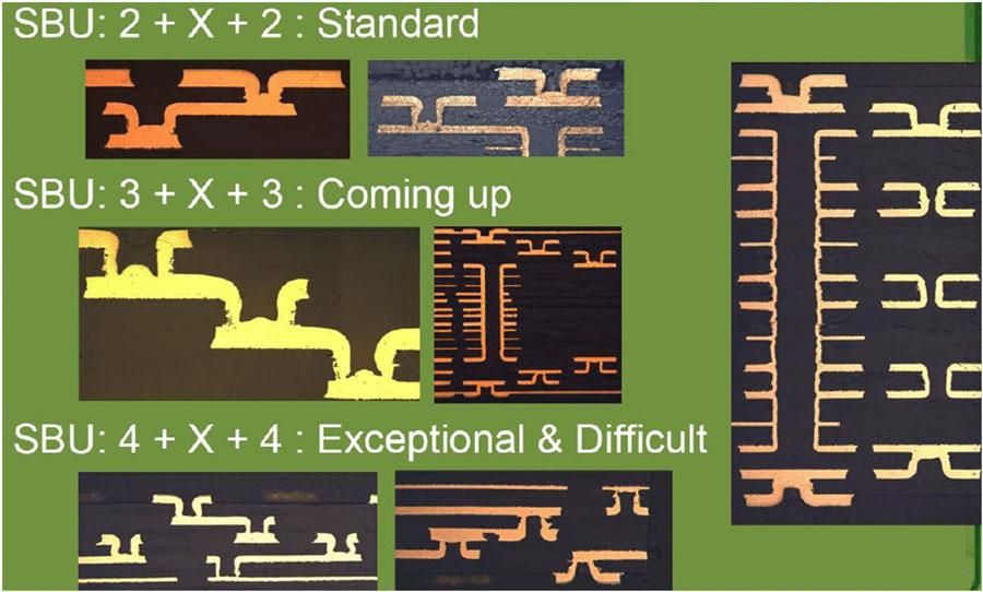
- 2 + n + 2 HDI pcb 2 layers for laser microvias, n layers for inner layers between the microvias.
- 3 + n + 3 HDI pcb 3 layers for laser microvias, n layers for inner layers between the microvias.
- 4 + n + 4 HDI pcb 4 layers for laser microvias, n layers for inner layers between the microvias.
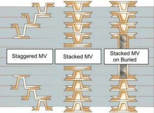
stagger microvia 1+1+..+1+n+1+1+..+1 Every Layer Interconnect PCB
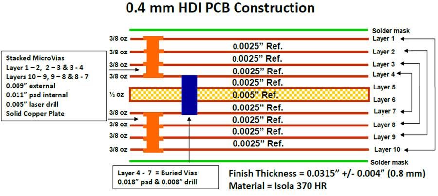
stacked Microvia hdi pcb
1+1+1+ ……+1+1+1 Stacked MicroVia 12 layers any layer HDI pcb
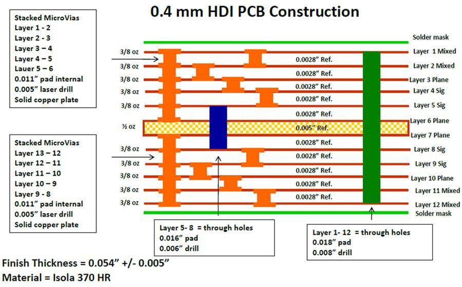
1+1+1+ n+1+1+1 Stacked MicroVia 10 layers pcb
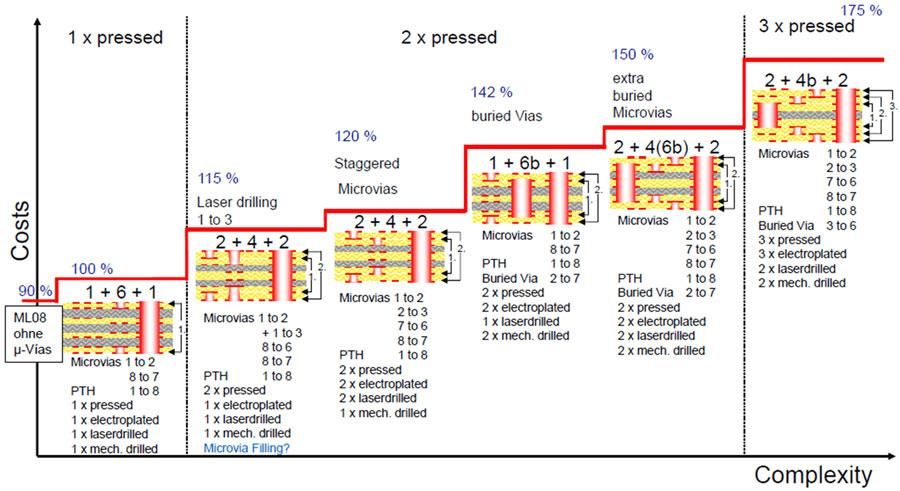
Cost of MicroVia HDI pcb Types
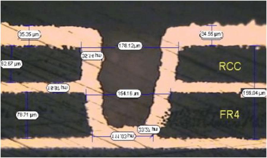
Plated Through High Aspect Ratio
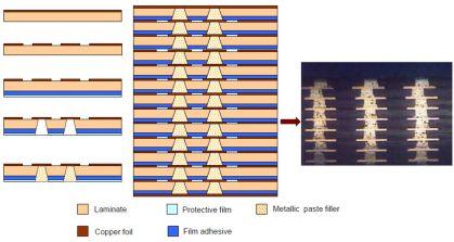
Lamination cycles up to multiple times for Stacked Microvia PCB
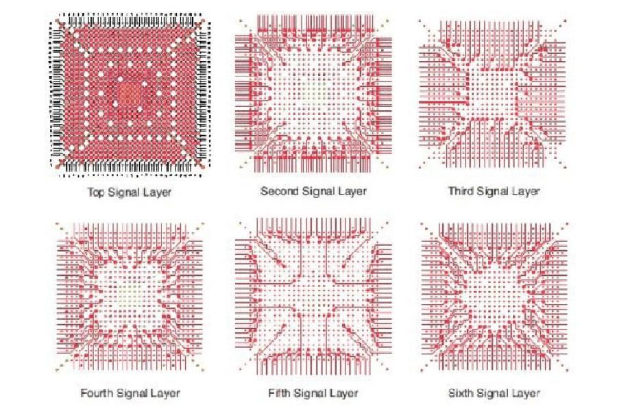
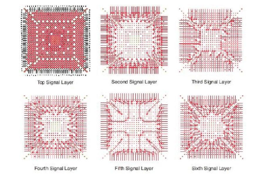
See also: How to BGA Fanout Routing in your HDI PCB
Today we are faced with a rapid reduction of PCB feature sizes due to the need for reduced form factor with fine pitch BGAs and small surface mount devices, and reduction or elimination of legacy components (replaced with ever smaller and denser packages).
With the advent of fine-pitch BGAs with many more rows of interconnects it is necessary to stack microvias to route surface signals to multiple layers below. Due to the tight spacing a single track between pads may not be feasible (due to greatly decreased line widths) so the ability to drop down another layer to fan out the signal is mandatory.
The flip side of this is the increased CTE mismatch between the solid copper microvia structure and the surrounding laminate. Laminate/copper stress cracks are more likely in stacks exceeding a 3 high structure (with typical PCB microvia diameters). Note that the CSP world has been doing this for many years successfully stacking 5 high +, but at much smaller diameters and dielectrics on different substrates.
Add to this an increasing number of designers entering the workforce without experience in required design technologies (blind & buried vias, sequential lamination, via-in-pad, laser microvias, etc.). Rather than provide specific routing examples such as those below I would prefer to focus on design minimums as these boundaries are routinely pushed or broken in modern PCB design.
At our in-house facility in China, we have successfully created so far HDI-SBU with sequencing reaching Any-Layer Interstitial Via Hole (ALIVH) in HDI pcb fabrication. We achieve this by applying a metallization technique to interconnect via holes (IVHs). This method not only offers stronger interconnection of stacked vias, but also achieves better thermal management, which significantly increases board reliability at severe circumstances.
We fabricate every piece of HDI SBUs in-house thanks to our complete range of advanced machines and equipment. Among the advanced equipment we own and operate include Laser Direct Imaging machines, which can provide reliable and repeatable 2/2 mils with the limited solder mask clearance of 1 mil. With such advanced equipment, we are also capable of fabricating probe cards, DUTs, and load boards for use in the semiconductors industry as well as burn-in boards of up to 50 layers on a 0.276-inch thick board with an aspect ratio of 40:1, metal core, and substrate PCBs containing 1.50 mils trace and space.
Concept to finish or problem specific, design engineers are available to assist our customers. Contact Hemeixinpcb to begin working with the design engineer most able to help you with your specific design needs. Please send your email to This email address is being protected from spambots. You need JavaScript enabled to view it. if you want to get some help.


