HDI Micro vias PCB
Why Blind Via HDI PCB
Microvias and stacked microvias can be found in High Density Interconnect circuit boards, also known as HDI PCBs, to enable complex interconnections in advanced designs.
Microvias, stacked microvias, and via-in-pad features allow miniaturization for higher functionality in less space and can accommodate large pin-count chips such as the ones used in cell phones and tablets. Microvias help reduce layer count in printed circuit board designs while enabling higher routing density and eliminating the need for through vias.
Consumers’ escalating demand for more features in their small and mobile electronics products, such as PDAs and cell phones, is driving a need for smaller feature sizes, process geometries, and pc boards. For engineers dealing with these desires, the need for HDI (high-density-interconnect) technology has become a reality. HemeixinPCB describes HDI PCB technology as a process that lets you produce a pc-board with through-hole, blind, or buried vias of less than 0.006 in. in diameter without using conventional drilling technology. Users of HDI technology must be able not only to assess and implement next-generation technology, but also to understand its boundaries in terms of layer stack up, via and microvia formation, feature size, and the primary differences between it and traditional pc-board technologies.
Blind via and Buried Via
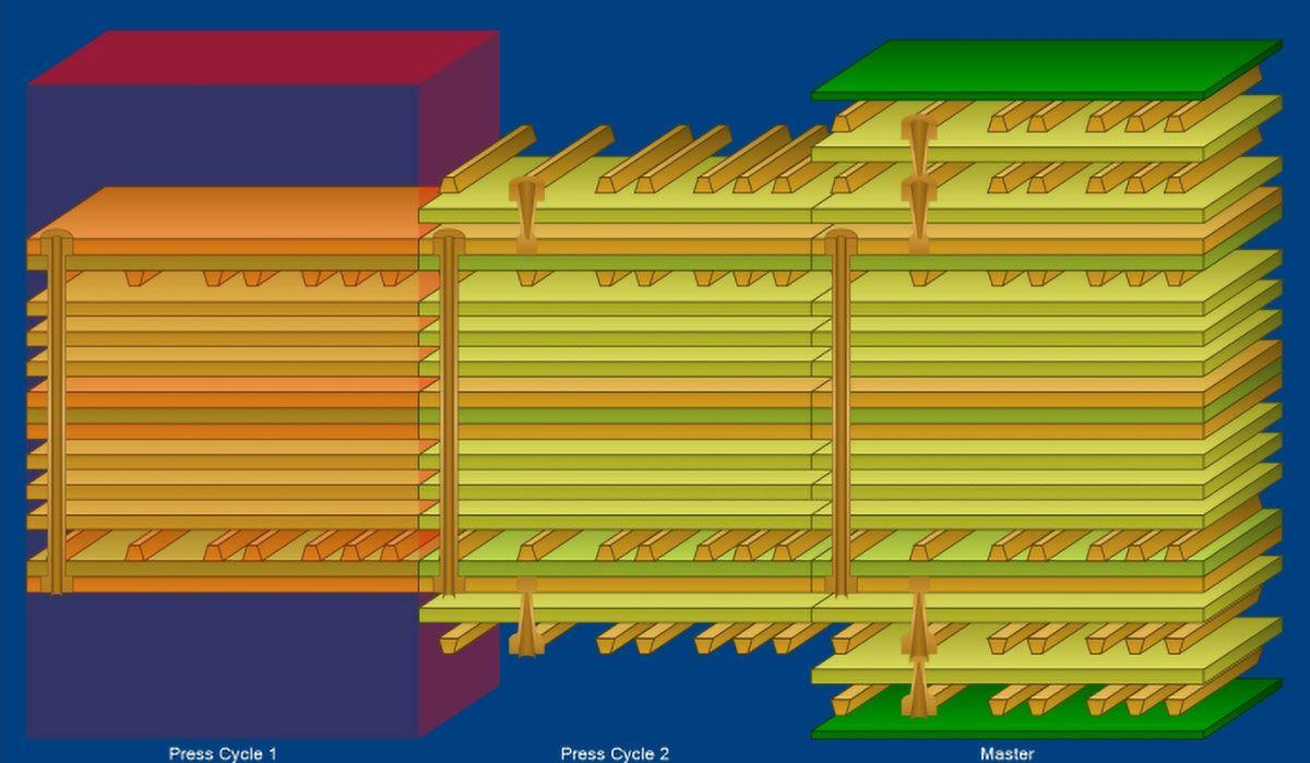
When PCB space is limited, or you’re working with tight plated through hole constraints, Blind and Buried Vias may be the answer.
Blind & Buried Via technology has played a pivotal role in squeezing more capability into a smaller space. By shortening vias to only pass through necessary layers, more surface area become available for components.
Blind and buried vias are used to connect between layers of a PCB where space is at a premium. A Blind Via connects an outer layer to one or more inner layers but does not go through the entire board. A Buried Via connects two or more inner layers but does not go through to an outer layer.
Key benefits include:
- Ability to meet the density constraints of lines and pads on a typical design without increasing the layer count or board size
- PCB aspect ratio reduction
Blind Via is a copper plated hole that connects only one outer layer to one or more inner layers. A blind via never goes all the way through a circuit board. In terms of design, blind vias are defined in a separate drill file.
Additional Benefit of Blind Vias:
Ability to widen BGA breakout channel (layer count reduction)
Buried Via is a copper plated hole that connects two or more inner layers, with no contact with the outer layer. It is impossible to detect a buried via as it is “buried” underneath the outer layer surfaces of a PCB. Buried vias also require a separate drill file.Buried Via
Additional Benefits of Buried Vias
- No impact to any trace or surface mount component on the top or bottom layers of the board.
- Trace or an SMD pad placement on the outer layers directly over the buried via (added space on outer layers)
What is a microvia hole?
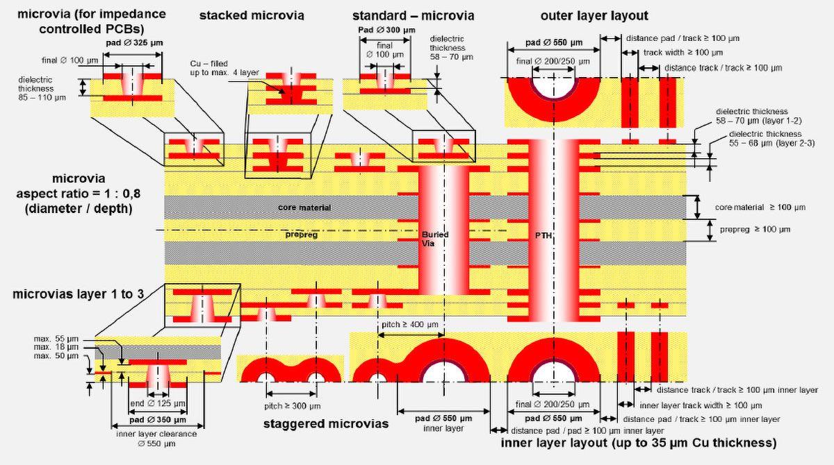
According to the new definition within IPC-T-50M a microvia is a blind structure with a maximum aspect ratio of 1:1, terminating on a target land with a total depth of no more than 0.25mm measured from the structure’s capture land foil to the target land.
The IPC-6012 also defines the structure of a Microvia.
- The Microvia is a blind structure with a maximum aspect ratio of 1:1 between hole diameter and depth, with a total depth of no more than 0.25 mm, when measured from the surface to the target pad or plane.
- Typically Hemeixin considers the dielectric thickness between surface and reference pad to be 60 – 80um.
- The diameter dimensions of the microvia have a range of 80-100 microns. The typical RATIO is between 0.6: 1 to 1: 1, ideal 0.8: 1
Layer stackup is a key differentiator of HDI-buildup technology. Engineers manufacture an HDI layer stack by depositing additional mirovia layers on traditional pc-board cores. The industry uses HDI construction types to describe the available layer stackups. Currently, three popular HDI-construction types are in use (See below picture). Type I construction comprises a conventional rigid or flexible pc-board core with any number of layers using through-hole vias and a single microvia layer fabricated on one or both sides of the core. Type II construction is similar, but you construct the vias in the core before adding the buildup microvia layers. Type III has at least two microvia layers on at least one of the core’s surfaces.
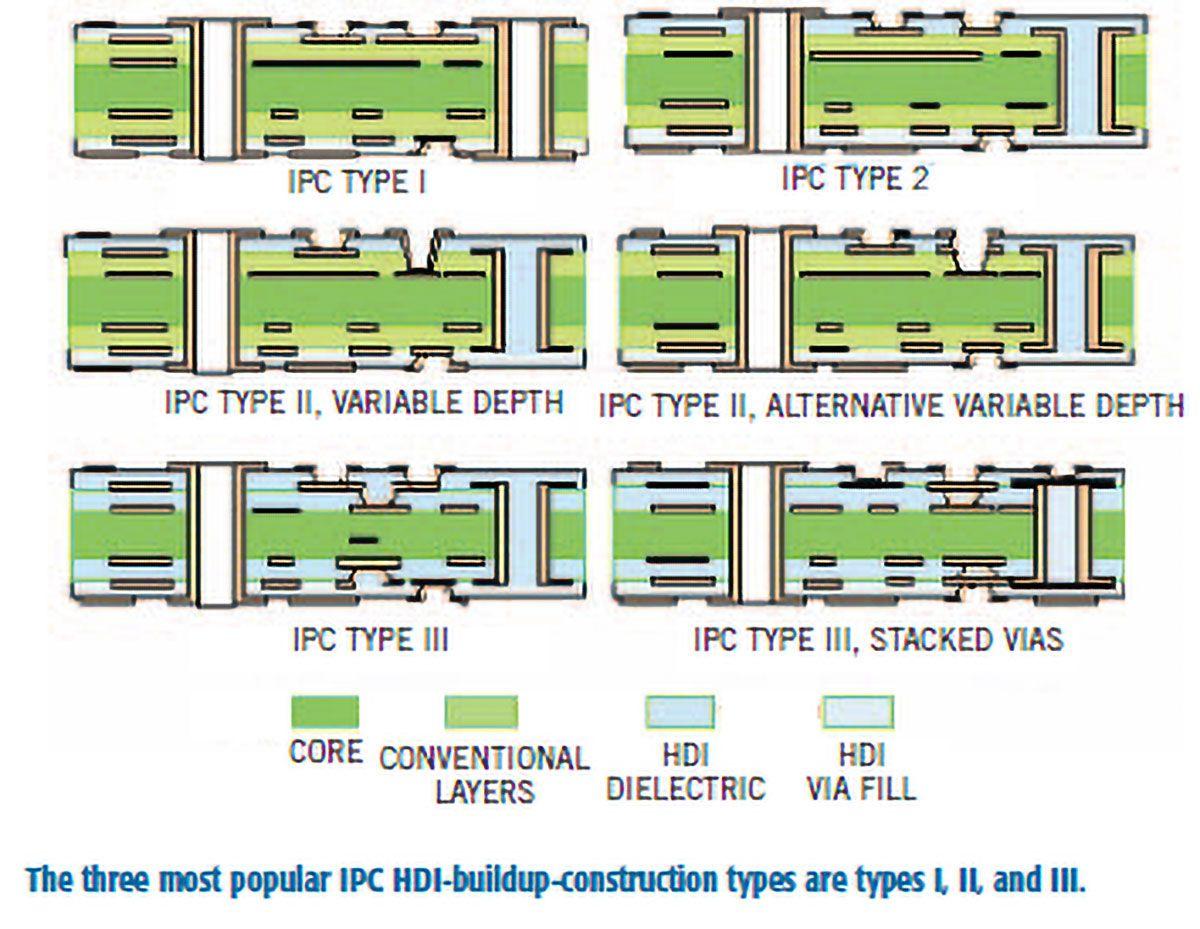
Several other construction types are available. Type IV construction comprises a “passive” core that can function as a nonelectrical shield or a thermal buffer. “Coreless” construction, which comprises a pair substrates laminated together, is Type V construction. Type VI construction, or colamination, occurs when you simultaneously form the interconnect and mechanical structure.
The multitude of layer stack up that engineers can derive by combining HDI-construction types and a varying number of layers has driven the need for a simple designation scheme to identify them. The identification method is straightforward. For example, a designation of “2 (C4) 2” indicates a layer-stack construction comprising a four-layer pc-board core (C4) with two HDI (buildup) layers on the top and two on the bottom. A designation of “2 (P) 2” indicates a Type IV construction with a passive core, two HDI layers on the top, and two HDI layers on the bottom.
Microvia and their effect on HDI PCB
A microvia is formed, not drilled like a traditional via. Engineers currently use several processes to produce microvias. Laser drilling, the most common technique, employs a focused laser beam to form the hole. Wet/dry etching is a mass-production process that creates all vias at the same time, regardless of the number or diameter of the holes. Photo imaging coats the base substrate with a dielectric layer. Engineers can also use conductive ink in microvia formation. In such a process, you form the microvias by laser drilling, photo imaging, or insulation displacement. You can also form microvias mechanically, using piercing, punching, abrasive blasting, or simple drilling. Each process produces different microvia hole shapes, such as cups, positive tapers, negative tapers, and straight walls (See below picture).
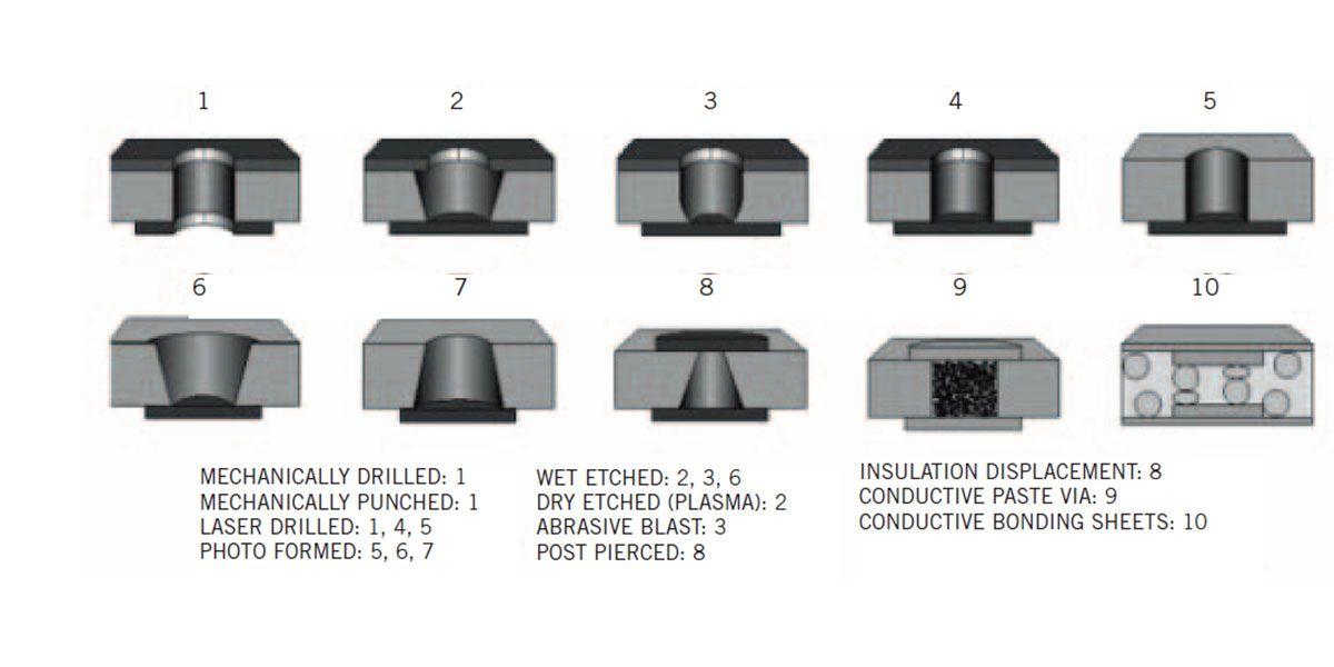
Each Microvia manufacturing process produces a different hole shape.
The advent of HDI technology and microvias has also led to a new vocabulary for via structures. The HDI Design Subcommittee of the IPC defines microvias as “formed blind and buried vias” that measure less than or equal to 0.15 mm and have pad diameters that measure less than or equal to 0.35 mm. In addition, designers use terms such as “capture land” (the area where the microvia originates) and “target land” (the area where the microvia ends) to describe the microvia pad sizes. A landless via has a land diameter that is the same size or smaller than the via diameter.
Currently, the size of microvias limits their current-carrying capability. Designers typically overcome this limitation by nesting several microvias in one large area called a plural via. Microvias that directly connect nonadjacent HDI-buildup layers are called skip vias. A variable-depth microvia is a microvia formed in one operation that penetrates two or more HDI-dielectric layers and terminates at one or more layers. Laser vias, conformal vias, filled vias, photo vias, and stud vias are microvias that derive their names from the processes used to form them.
Each HDI pcb construction type allows the use of different combinations of “standard” vias and microvia structures. Type I construction lets you use blind, one-layer-deep microvias and a standard through-hole via. The standard via spans all layers in the stack including the HDI-buildup layers. Type II construction is similar to Type I but adds a buried via that spans all the layers of the pc-board core. Type III adds yet more complexity to the via structures, allowing the use of buried, stacked, staggered, and variable-depth microvias. These many via structures can add a significant level of complexity to the layout of HDI-buildup designs.


