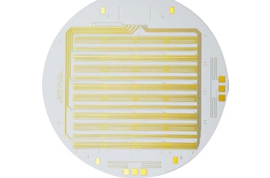
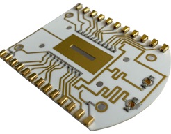
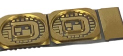
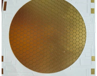
Ceramic PCB
 Ceramic PCB Manufacturing
 Ceramic PCB Manufacturing
What is Ceramic Substrate PCB?
For PCBs placed in environments of high pressure or high temperature, traditional PCB substrate materials may exhibit flaws in extreme conditions. However, ceramic PCB substrate material is suitable for high temperature and pressure as well as corrosive or vibrational circuit conditions. Ceramic PCBs have a high thermal conductivity as well as coefficient of thermal expansion. These PCBs are most suitable for high power density circuit designs that are used in extreme conditions, especially in the aerospace and automotive industries.
Ceramic PCBs are made from a range of ceramic materials. The thermal conductivity and coefficient of thermal expansion (CTE) are the main two properties to focus on when selecting ceramic materials. The ceramic materials used in PCBs refer to a class of substrate materials such as aluminum nitride (AlN), alumina (Al2O3), beryllium oxide (BeO), silicon carbide (SiC), and boron nitride (BN). These ceramic materials share similar chemical and physical properties. Below, we will explore the properties of three common ceramic materials.
Ceramic PCB Material Available
-
Alumina (Al2O3) - The mechanical strength, chemical stability, thermal conductivity, and electrical properties of Al2O3 are advantageous compared to other oxide ceramics. The abundance of raw material makes alumina the most commonly used ceramic substrate material. Al2O3 ceramic PCBs are used in automobile sensor circuits, shock absorbers, and engines. The high thermal stability of Al2O3 ceramic PCBs improves the performance and thermal efficiency of the circuits used in automobiles.
-
Aluminum Nitride (AlN) - The high thermal conductivity and coefficient of expansion are two properties that make AlN noteworthy as a substrate material in the PCB industry. The thermal conductivity of AlN varies in the range of 170 W/mK to 220W/mK. The CTE of AlN ceramic matches with silicon semiconductor chips, which establishes a good bonding between the two, thus making their assembly reliable. AIN is used in sensor circuits in automobiles, as it can withstand extreme temperatures, corrosion, and vibration while providing efficient, accurate, and sensitive sensor signals.
-
Beryllium Oxide (BeO) - BeO is a ceramic PCB substrate material with a thermal conductivity around nine times that of Al2O3 and greater than metal aluminum. BeO showcases better chemical stability than AlN and high electrical isolation comparable with Al2O3e. BeO is used in applications where the PCB is subjected to high temperatures or in high-density PCBs facing space limitations to provide air or liquid cooling.
Aluminum oxide PCB (Al2O3 or Alumina) solutions
Aluminum oxide PCB (Al2O3 or Alumina) is today the most widely used ceramic printed circuit board and submounts. This is thanks to its good material properties, namely good thermal conductivity, low CTE (coefficient of thermal expansion), resistance to chemical hazards and hermeticity in combination with a relatively low cost and a more easy handling. Applications include for example cooling and heating modules, LED boards, medical circuits, sensor modules, and high-frequency devices.
The main reasons Alumina is chosen over other printed circuit boards is:
- Higher operating temperature up to 350ºC (using thick film printing)
- Lower expansion coefficient (6-8 ppm/ºC) matching components
- Good thermal properties (22-24 W/mK)
- Superior high-frequency performance
- Smaller package size due to integration and multi-layer possibilities
- High wear and chemical hazards resistance
- Hermetic packages possible, 0% water absorption
- Good light reflection due to white color.
- Limited to no outgassing
- Strong rigid material
At Hemeixin, we supply both Aluminum Oxide PCB (Al2O3 96%) made by thick film process (Silver metalization) as well as Direct Plated Copper Technologies (DPC), with copper tracks and pads.
Aluminum Nitride PCB solutions
Aluminum Nitride PCB (AlN) is one of the best performing circuits solutions today for high current or high temperature electronics. Thanks to its incredible thermal conductivity (170 W/mK) and dielectric strength combined with its low thermal expansion (CTE <4 ppm/C) it is used today in many application ranging from high power LEDs and lasers to high current switches, ultra low temperature vacuum chamber electronics (e.g. quantum computing) and many many more … . Furthermore it has all the additional benefits other ceramic material have like rigidity, resistance against environments & chemical hazards and 0% water absorption.
The main reasons Aluminum Nitride is chosen over other printed circuit boards is:
- Superior thermal conductivity 170W/mK
- Strong dielectric
- High operating temperature >350ºC possible
- Low expansion coefficient <4 ppm/C
- Smaller package size due to integration
- Hermetic packages possible, 0% water absorption
- Limited to no outgassing
At Hemeixin, we supply both Aluminium Nitride PCB (AlN) processed by thick film process (Silver/silver palladium metalization) as well as Direct Plated Copper Technologies (DPC), with copper tracks and pads.
Ceramic PCB Design Guidelines
1. Ceramic PCB Material
|
Item |
Spec |
|
Standard material |
AL2O3(92%,95%,96%) AIN(thermal conductivity 170-200W) |
|
Material need special control |
AL2O3(99%) AIN(thermal conductivity 200-230W) |
|
Material need evaluation |
Zirconia,Beryllium oxide,silicon nitride,quartz glass |
2. Ceramic PCB Material specification
|
Item |
Spec |
|
Common material size |
50mmX50mm 120mmX120mm 140mmX190mm |
|
Special material size |
Materials out of spec of above mentioned size need evaluation. |
3. Ceramic PCB Material thickness
|
Substrate type |
Substrate thickness(mm) |
|
AL2O3\AIN ceramic pcb |
0.38, 0.5, 0.635, 0.8, 1.0,1.2,1.5, 1.8, 2.0,2.5, 3.0 |
|
Material need special control |
AL2O3 0.125,0.2,0.25,0.3 AIN 0.25,0.3 |
|
Material need evaluation |
Materials out of spec of above mentioned size need evaluation. |
4. Ceramic PCB Laser drill
|
Board thickness(mm) |
Standard(um) |
In advance min hole size(um) |
|
0.25 |
80 |
60 |
|
0.3 |
80 |
60 |
|
0.38 |
100 |
80 |
|
0.5 |
120 |
100 |
|
0.635 |
180 |
150 |
|
0.8 |
200 |
180 |
|
1.0 |
250 |
200 |
|
1.2 |
300 |
250 |
|
1.5 |
380 |
300 |
|
2.0 |
500 |
300 |
|
When board thickness >2.5mm, board thickness/hole size ≧4:1,or min hole size out of above spec,evaluation is needed. |
||
|
Hole to hole space:0.25mm or larger. |
||
5. Line with/Line space
|
Copper thickness |
Standard |
|
|
18(um) |
60(um) |
|
|
30(um) |
≥75(um) |
|
|
60(um) |
≥100(um) |
|
|
80(um) |
120(um) |
|
|
Evaluation is needed when line width/space smaller than 50um, or line width/space smaller than above data. |
||
6. Solder mask and silkscreen
|
Item |
Standard |
In advance |
Need evaluation |
|
Solder mask color |
Green, blue, yellow, red, light green, matte green, matte blue, matte black |
transparent, gray,Neon green |
Other colors |
|
Solder mask dam |
Green: 120um Other colors:150um |
Green:100um Other colors:120um |
Smaller width than left columns. |
|
Silkscreen color |
Black, white |
Same as standard solder mask colors. |
|
|
Silkscreen height |
≥800(um) |
≥650(um) |
Smaller height than left columns. |
7. Surface finish and thickness
|
Standard surface finish and plating thickness |
Special controlled surface finish and plating thickness |
|
Hard gold plating(um) NI:3.05-5.08, AU:0.127-2 ENEPIG(um) NI:3.05-5.08, PD:0.025-0.2, AU:0.025-0.2 Immersion silver: 0.2-1 Immersion Tin: OSP: 0.2-0.6 HASL (LF) |
ENIG:(um) NI:5.08-6.35, AU:0.2-0.76 Hard gold plating(um) NI:5.08-6.35, AU:2-4 ENEPIG(um) NI:5.08-6.35, PD:0.2-0.5, AU:0.2-0.76 |
|
Evaluation is needed when hard gold plating area bigger than 50%, silver plating and other plating thickness exceed above parameters. |
|
8. Outline process
|
Process |
Tolerance |
Max board size |
|
Laser cutting |
±0.1mm |
130*140mm |
|
Water Jet Cutting |
±0.1mm |
130*140mm |
|
Evaluation is needed when tolerance exceed above parameters. |
||
|
Item |
Requirement |
|
Laser pre cutting(lineation) |
Standard technique, board thickness 0.5mm, pre-cut depth15-30%. |
|
Special controlled, board thickness 0.38mm, pre-cut depth 10-15%. |
|
|
Evaluatoin is needed when board thickness less than 0.38mm, and laser pre cutting is required. |
|
Item |
Requirement |
|
Laser cutting |
Standard technique: board to board space ≥0.25mm Special controlled: board to board space ≥0.2mm |
|
Water Jet Cutting |
Depends on blade width |
|
Others need evaluation. |
|
Ceramic PCB Capabilities
Compared with regular substrates like glass epoxy (FR4) or aluminium (Al), the ceramic substrate is an ultra-thin composite structure. It offers superb electrical insulation, high thermal conductivity, high adhesion strength. Because of these characteristics, a ceramic substrate PCB has higher current carrying capacity, while it is possible to etch it just like a regular board can. With harsh weather resistance capabilities, ceramic PCBs are suitable for harsh outdoor environments. Ceramic PCBs are eminently suitable for product that generate high heat, such as solar energy equipment and high-brightness LEDs do. Alumina PCB and Aluminum Nitride PCB solutions below:
Direct plated copper (DPC) Technology
|
DPC Technology |
|||
|
Process |
Item |
MP capability |
|
|
Standard |
Layers |
1-2L |
|
|
Base material thickness |
0.15-2.5mm |
||
|
Board thickness tolerance |
±10% |
||
|
Warpage |
≤0.7% |
||
|
Laser drill |
Min laser hole size |
0.06mm |
|
|
Hole tolerance |
PTH |
±0.075mm |
|
|
NPTH |
±0.025mm |
||
|
Electroplating |
aspect ratio |
Through hole |
4:1 |
|
Electroplating filling via |
Filling via size |
0.07-0.25mm |
|
|
Layout design |
Max base copper |
Outer layer |
≤100um |
|
Line width/space (outer layer) |
Copper thickness 10-35um |
3/3mil |
|
|
Copper thickness 35-100um |
4/4mil |
||
|
Line width tolerance |
Line width≥10mil |
±2mil |
|
|
Line width<10mil |
±20% |
||
|
Pad size tolerance |
Pad size≥12mil |
≥±10% |
|
|
Box dam height |
150um-1200um |
±50um |
|
|
Outline |
Laser cutting or water jet cutting |
Outline tolerance |
≤±100um |
|
Max board size |
130*180mm |
||
|
Surface finish |
Hard gold plating |
Gold thickness |
0.127-2um |
|
Nickel thickness |
3.05-5.08um |
||
|
ENIG |
Gold thickness |
0.025-0.76um |
|
|
Nickel thickness |
3.05-5.08um |
||
|
ENEPIG |
Gold thickness |
0.025-0.76um |
|
|
Palladium thickness |
0.025-0.2um |
||
|
Nickel thickness |
3.05-5.08um |
||
|
OSP |
Film thickness |
0.2-0.6um |
|
|
Immersion silver |
Silver thickness |
0.2-1um |
|
Direct Bonded Copper and Active Metal Brazing Technology
|
DBC&AMB technology |
|||
|
Process |
Item |
MP capability |
|
|
Standard |
Layers |
1-2L |
|
|
Base material thickness |
0.38-1.0mm |
||
|
Board thickness tolerance |
±10% |
||
|
Warpage |
≤0.7% |
||
|
Laser drill |
Min laser hole size |
0.15mm |
|
|
Hole tolerance |
PTH |
/ |
|
|
NPTH |
±0.1mm |
||
|
Aspect ratio |
Through hole |
4:1 |
|
|
Layout design |
Max base copper thickness |
Outer layer |
127-400um |
|
Copper thickness |
0.127mm |
Space: 0.30mm |
|
|
0.20mm |
Space: 0.35mm |
||
|
0.25mm |
Space: 0.40mm |
||
|
0.30mm |
Space: 0.45mm |
||
|
0.40mm |
Space: 0.55mm |
||
|
Line width tolerance |
Line width≥10mil |
±2mil |
|
|
Line width<10mil |
±20% |
||
|
Pad size tolerance |
Pad size≥15mil |
≥±10% |
|
|
Outline process |
Laser cutting or water jet cutting |
Outline tolerance |
≤±100um |
|
Max board size |
130*180mm |
||
|
Surface finish |
ENIG |
Gold thickness |
0.025-0.76um |
|
Nickel thickness |
3.05-5.08um |
||
|
ENEPIG |
Gold thickness |
0.025-0.76um |
|
|
Palladium thickness |
0.025-0.2um |
||
|
Nickel thickness |
3.05-5.08um |
||
|
OSP |
Film thickness |
0.2-0.6um |
|
|
Immersion silver |
Silver thickness |
0.2-1um |
|
Types of Ceramic Circuit Board Based on Manufacturing Processes
PCB manufacturers use several methods to form boards with ceramic substrates: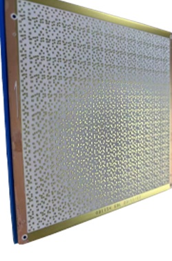
Direct Bonded Copper (DBC): The manufacturer deposits a layer of copper on the ceramic material using a eutectic solution of copper and oxygen. A copper deposit forms on the ceramic when there is an optimum proportion of oxygen in the solution and the temperature is between 1065 and 1083 °C. The ceramic material reacts with the eutectic liquid to form copper-aluminum oxide.
Direct Plate Copper (DPC): Manufacturers use professional film manufacturing technology or vacuum techniques for DPC. They clean the ceramic material and bond it with a copper composite layer. They expose the structure to the required trace pattern and develop it with yellow light lithography before etching. After removing the film, the manufacturer increases the copper thickness by electroplating it. They remove the photo-resist, revealing the completed circuit.
Laser Activation Metallization (LAM): In this method, manufacturers use a high-power laser beam to ionize the copper metal and ceramic. The resulting heat causes the copper and ceramic to bond firmly. These boards have superior characteristics, such as:
- High-Temperature endurance
- Better insulation
- Consistent coefficient of thermal expansion
- High thermal conductivity
- Customizable conductor thickness
- High density assembly
- low high-frequency losses
- No oxide layer formation
- Low organic impurities
- Low electrical resistance
Thick Film Ceramic: These involve applying a paste of gold conductor material on the ceramic base material. The manufacturer then bakes them at a temperature of about 1000 °C. However, the high cost of gold conductor paste makes this variety of PCBs non-popular.
The main benefits of thick film ceramic as compared to traditional PCBs is the presence of gold does not allow the copper to oxidize. Although the minimum number of layers in a ceramic PCB is two, depending on the requirement, there can be several layers.
What Are the Types of Ceramic Printed Circuit Board?
Ceramic Printed Circuit Boards (PCBs) come in various types and configurations, each designed to cater to specific applications and performance requirements. Here are some common types of ceramic PCBs: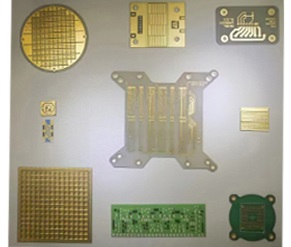
- Single-Layer Ceramic PCBs: These are basic ceramic PCBs with a single conductive layer on a ceramic substrate. They are often used for simple applications where high thermal conductivity is needed but complex circuitry is not required.
- Multilayer Ceramic PCBs: These PCBs consist of multiple layers of ceramic substrates, with conductive traces and vias connecting the different layers. Multilayer ceramic PCBs are suitable for complex circuit designs, high-density interconnects, and applications requiring signal integrity.
- Thick Film Ceramic PCBs: In this type, thick film technology is used to create conductive and resistive traces on ceramic substrates. Thick film ceramic PCBs are known for their durability, making them suitable for applications in harsh environments like automotive and industrial settings.
- Thin Film Ceramic PCBs: Thin film technology involves depositing thin layers of conductive and insulating materials onto the ceramic substrate. Thin film ceramic PCBs offer precise electrical properties and are commonly used in high-frequency applications, such as RF and microwave devices.
- Hybrid Ceramic PCBs: These PCBs combine ceramic materials with other materials, such as organic substrates or metal cores. The hybrid approach allows engineers to balance the benefits of ceramics with the advantages of other materials, such as cost-effectiveness or specific thermal properties.
- Alumina (Al2O3) Ceramic PCBs: Alumina ceramic PCBs are made from aluminum oxide and are known for their high thermal conductivity, electrical insulation, and mechanical strength. They are suitable for various applications, including power electronics, LED modules, and high-power RF devices.
- Aluminum Nitride (AlN) Ceramic PCBs: Aluminum nitride ceramic PCBs offer even higher thermal conductivity than alumina, making them suitable for applications where efficient heat dissipation is critical. They are often used in high-power electronic devices and LEDs.
- Beryllium Oxide (BeO) Ceramic PCBs: Beryllium oxide ceramic PCBs are characterized by extremely high thermal conductivity and are used in applications that demand efficient heat dissipation, such as high-power RF amplifiers.
- Silicon Carbide (SiC) Ceramic PCBs: Silicon carbide ceramic PCBs are known for their excellent thermal and electrical properties, as well as their ability to withstand high temperatures and harsh environments. They are used in high-temperature electronics and power electronics.
- LTCC (Low-Temperature Co-fired Ceramic) PCBs: LTCC technology involves co-firing multiple layers of ceramic substrates at relatively low temperatures. LTCC ceramic PCBs are used in RF modules, sensors, and other miniaturized devices.
Why are Ceramic PCB Board used?
Ceramic PCBs offer several properties that enhance electronics’ durability, reliability, and performance. These include: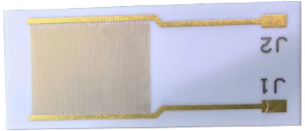
- Thermal Conductivity: Ceramics have excellent thermal conductivity, aiding in heat dissipation from electronic components, preventing overheating, and ensuring long-term reliability
- Dielectric Properties: Ceramics possess high dielectric constants, making them suitable for high-frequency applications and efficient signal transmission
- Electrical Insulation: Ceramics are excellent electrical insulators, preventing electrical leakage and ensuring the isolation of different circuit components
- Mechanical Strength: Ceramics are mechanically robust, with high tensile and compressive strength, making them resistant to physical damage
- Chemical Resistance: They are generally resistant to chemicals and environmental factors, ensuring the durability of electronic systems
What type of applications are Ceramic PCBs used in?
Ceramic PCBs are used in electronic devices and systems where exceptional thermal management, high-frequency performance, and reliability are crucial. Common uses include:
- High-Frequency Electronics: Such as RF (radio frequency) devices, microwave circuits, and radar systems. Ceramic PCBs have low signal loss and high dielectric constants, making them ideal for these applications
- LED Lighting: Ceramic PCBs serve as substrates for LED modules. Their efficient heat dissipation capability helps maintain LED light longevity and performance
- Power Electronics: In power electronics, where efficient heat dissipation is essential, ceramic PCBs can handle high temperatures and provide thermal stability
- Aerospace and Defense: these industries use ceramic PCBs in radar systems, communication equipment, and missile guidance systems due to their reliability and high-frequency capabilities
- Medical Devices: Some medical devices, like medical imaging equipment and wireless communication devices, use ceramic PCBs for superior performance and durability
Ceramic PCB Fabrication Process
The fabrication process of Ceramic Printed Circuit Boards (PCBs) involves several steps that transform ceramic substrates into functional electronic circuits. The process may vary depending on the specific type of ceramic PCB and the manufacturer's capabilities, but here is a general overview of the steps involved in the fabrication of ceramic PCBs:
1. Design and Layout: The process begins with the design of the circuit layout using computer-aided design (CAD) software. Components, traces, vias, and other elements are placed and routed on the layout, considering factors such as thermal management and signal integrity.
2. Substrate Preparation: Ceramic substrates are chosen based on the application's requirements, such as thermal conductivity and electrical properties. The ceramic substrate is prepared by cutting, shaping, and polishing to the desired dimensions and surface finish.
3. Layer Preparation (for Multilayer PCBs): For multilayer ceramic PCBs, individual ceramic layers are prepared and fabricated. These layers will eventually be stacked and interconnected. Each layer may undergo processes such as screen printing, where conductive and insulating pastes are applied to create circuit traces and insulation layers.
4. Conductive Layer Deposition: Conductor materials, often metal pastes containing silver or gold particles, are applied to the substrate using techniques like screen printing or inkjet printing. These conductive traces will carry electrical signals between components.
5. Via Drilling and Filling: Vias, which are small holes that connect different layers of the PCB, are drilled using laser or mechanical drilling techniques. The vias are then filled with conductive or non-conductive materials to establish connections between layers.
6. Firing or Sintering: The ceramic substrate with applied conductive materials is fired in a high-temperature furnace. This process sinters the ceramic and fuses the conductive materials, creating a solid and durable circuit structure.
7. Additional Layering (for Multilayer PCBs): The process of applying conductive traces, insulating layers, and vias is repeated for each layer in the multilayer stack.
8. Component Attachment: Components, such as surface-mounted devices (SMDs), are attached to the ceramic PCB using soldering or specialized adhesives. Due to the high thermal conductivity of ceramics, specific soldering techniques may be required to ensure proper bonding.
9. Testing and Inspection: The assembled ceramic PCB is subjected to various tests, including continuity checks, electrical testing, and potentially environmental testing. Inspection processes help identify defects and ensure the PCB's functionality and reliability.
10. Finishing and Coating: Protective coatings or encapsulants can be applied to safeguard the PCB from environmental factors such as moisture, chemicals, and temperature variations.
11. Final Testing: The completed ceramic circuit board undergoes final functional testing to ensure it meets the specified requirements and operates correctly.
12. Packaging and Delivery: Once the ceramic PCB passes all tests and inspections, it is packaged and prepared for delivery to the customer or further integration into electronic devices.
Ceramic PCB Manufacturer
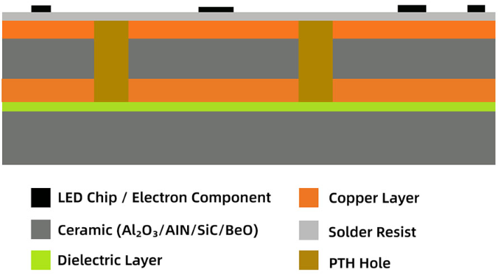
Printed circuit boards with ceramic substrates are boards made with a special process where the manufacturer bonds the copper foil directly to the surface of a ceramic substrate made of Aluminum Nitride (AlN) or Alumina (Al2O3). According to Hemeixin., the bonding takes place at a high temperature, and the copper foil may be present on one or both sides of the ceramic substrate, depending on whether the board is single-sided, double-sided or multilayer.
A Ceramic Printed Circuit Board uses ceramics as its substrate material. Ceramics are known for their exceptional electrical, mechanical, and thermal properties, making them suitable for various applications.
Ceramic PCBs utilize ceramics as substrates, known for exceptional properties like thermal conductivity and electrical insulation. These PCBs are used in high-frequency electronics, LED lighting, power electronics, aerospace, and medical devices. While ceramics insulate electricity well, they are brittle, and manufacturing can be complex. A common issue is their susceptibility to cracking under mechanical stress or temperature changes.