
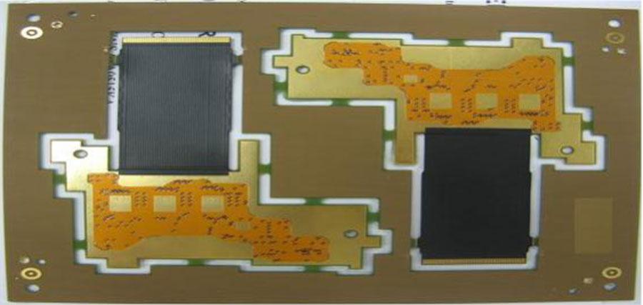
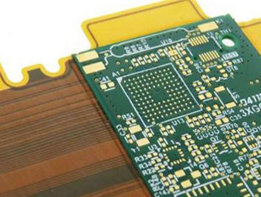
Rigid flex PCB design guidelines
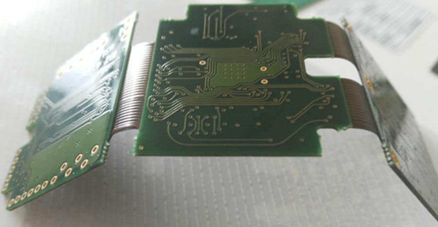
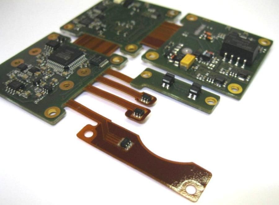
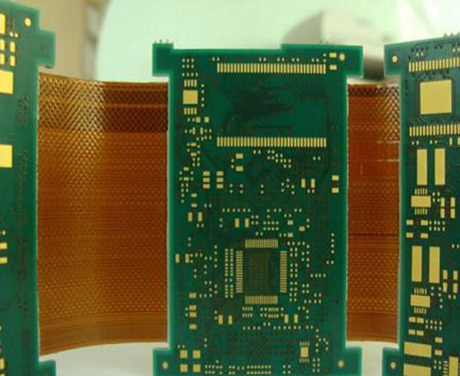
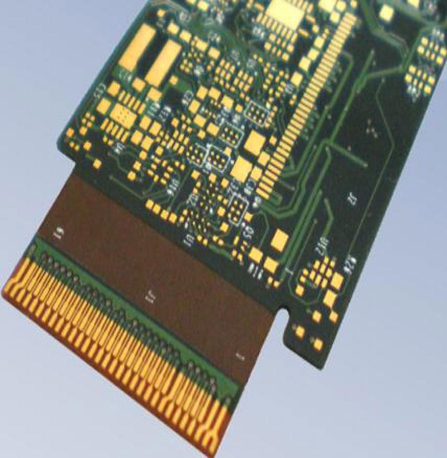
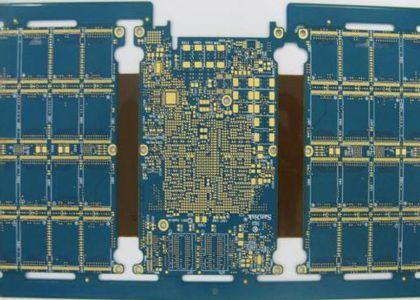
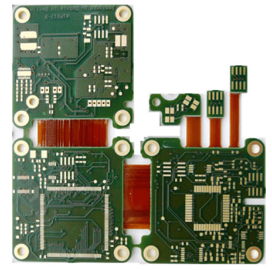
The use of rigid-flexible PCBs opens for many applications completely new possibilities and advantages regarding signal transmission, size, stability and long-term reliability.
In recent years, Hemeixinpcb has accumulated extensive expertise in costumer projects and commissions of the widest variety of designs and applications, from Aerospace to Medical devices and currently it supplies more than 1000 customers. With the broad range of technology we offer, you can make the best possible selection for any requirements in terms of performance and costs.
For first time designers and engineers it is a good idea to become familiar with the specifications that have reference to rigid-flex pcb manufacturing.
Below rigid flex pcb guildelines including these contents:
-
Rigid-Flex PCB board standard stack up
-
Rigid-Flex PCB base materials
-
Rigid Flexible PCB Design Guides and Rules
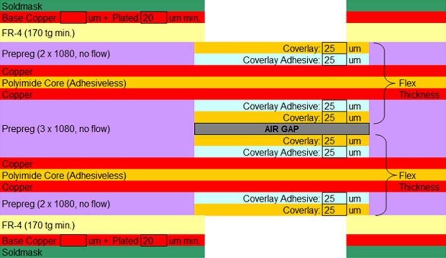
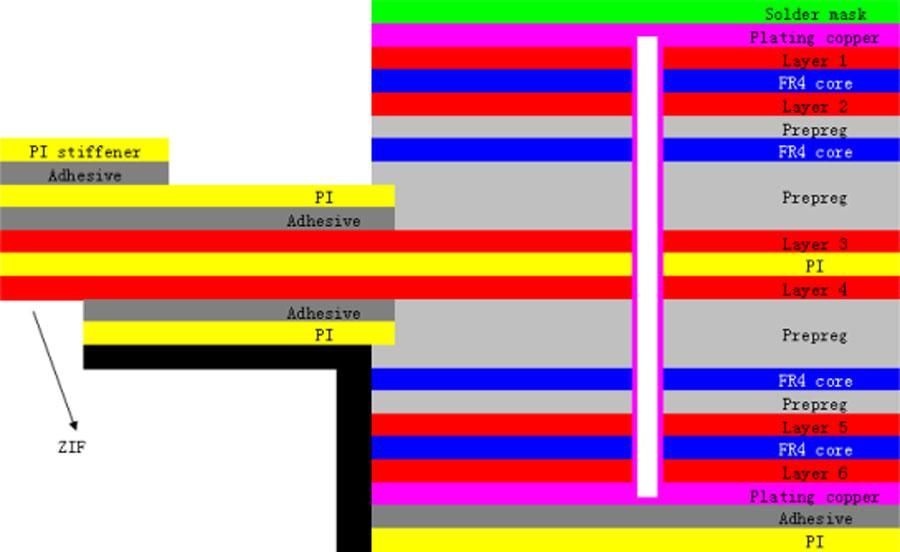
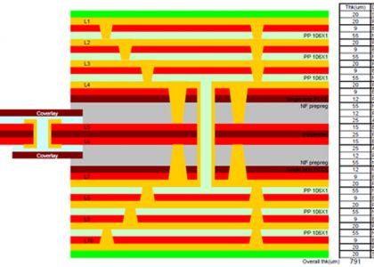
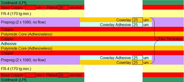
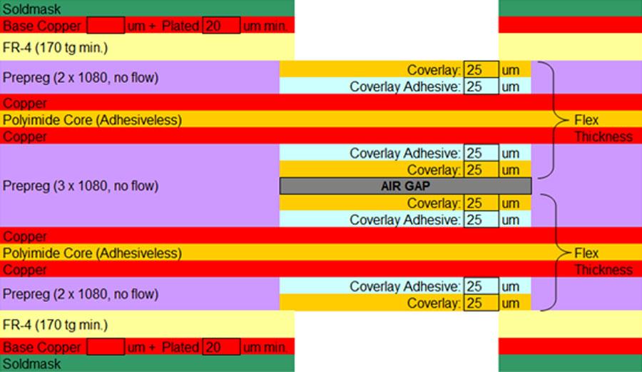
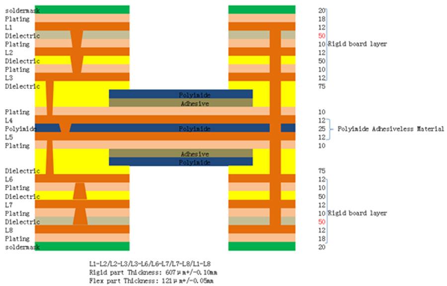
Rigid flex pcb fabrication layer up
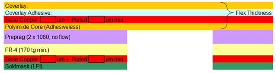
2 layer rigid flex pcb layer up
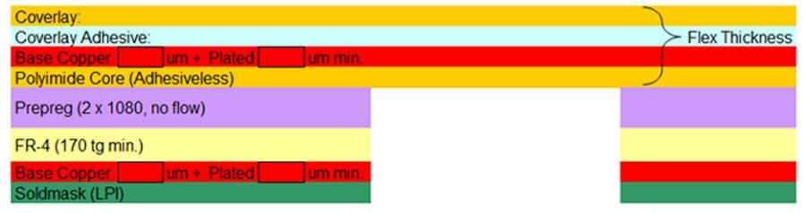
3 layer rigid flex pcb layer up

4 layer rigid flex pcb layer up

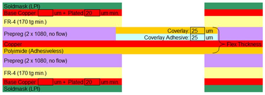
5 layer rigid flex pcb layer up
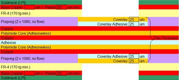

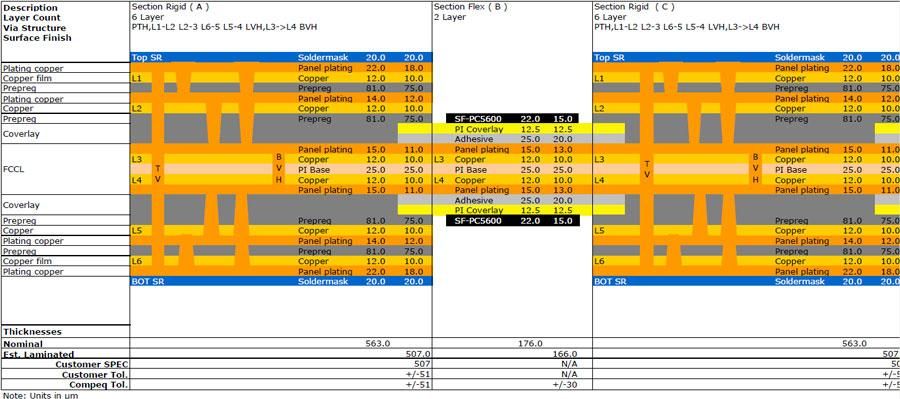
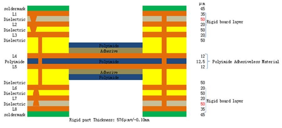
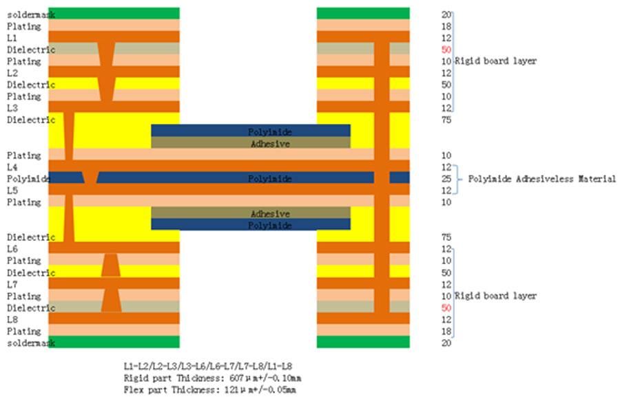
6 layer rigid flex pcb layer up

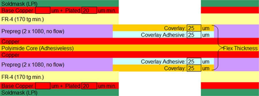
6 layer Any layer HDI rigid flex pcb layer up
8 layer HDI Blind and buried via rigid flex pcb layer up

8 layer Any layer HDI rigid flex pcb layer up
12 layer Any layer HDI rigid flex pcb layer up and ZIF contacts
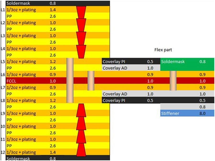
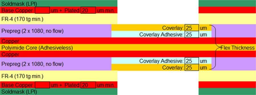
Rigid Flex PCB base material
This table lists the materials and material thicknesses that Hemeixinpcb has available. Hemeixinpcb’s standard materials are in boldface. If the material or thickness is not listed, send email to This email address is being protected from spambots. You need JavaScript enabled to view it..
| Material | Sizes/thickness |
|---|---|
| Flex material-Kapton and other polyimide films | 1/2 mil(12.5μm), 1 mil(25μm), 2 mil(50μm), 3 mil(75μm), 5 mil(125μm). Example: AP 8515R, AP 9111R, AP 8525R, AP 9121R, AP 9222R, AP 8535R, AP 9131R, AP 9232R, AP 8545R, AP 9141R. ect… |
| Coverlay | 1 mil(25μm), 2 mil(50μm), 3 mil(75μm), Example: FR0110, FR0120, ect… |
| Rigid material- FR4 | Variety of thicknesses between 0.003″ (0.08mm)and 0.125″ (3.18mm) |
| Copper weight | 1/4 oz. (9μm), 1/3 oz. (12μm), 1/2 oz. (18μm), 1 oz (35μm), 2 oz. (71μm), 3 oz. (107μm), 5 oz. (175μm), 7 oz (254μm), 10 oz. (356μm) |
| Adhesive | 1/2 mil (12.5μm), 1 mil (25μm), 2 mil (50μm), 3 mil (75μm), 4 mil (100μm) |
| Pressure-sensitive adhesive (PSA) | 1 mil (25μm), 2 mil (50μm), 4 mil (100μm), 5 mil (125μm) |
| Stiffener | Copper, Aluminum, and other metals. Variety of thicknesses available |
| Stainless steel up to 20 mils(500μm) | |
| Polyimide thickness between 1/2 mil (12.5μm), 1 mil (25μm), 2 mil (50μm), 3mil (75μm), 4 mil (100μm), 5 mil (125μm), 6mil (150μm), 7 mil (175μm), 8 mil (200μm), 9 mil (225μm), 10mil (250μm) | |
| FR-4 thickness between 0.005″ (0.13mm)and 0.125″ (3.18mm) |
Rigid-flex PCB Design Guides and Rules
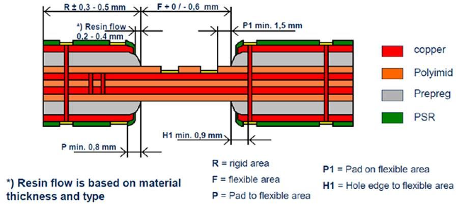
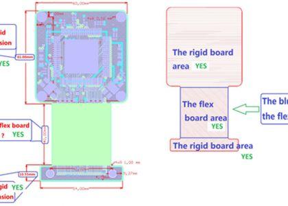
1. Distance Design Guides and Rules
-
Distance from holes to flex area≥0.9mm
-
Length of flex area≥2.0mm
-
Rigid PCB part of the pad to flexible area≥0.8mm
-
Flexible area of the pad to rigid PCB part≥1.5mm
2. Additional rigid flex pcb fabrication Considerations
Designs that have one or more of the following may require the use of coverlay throughout in specific areas or layers:
-
ZIF finger area Polyimide stiffener(s)
-
FR4 component area rigidizing stiffener(s)
-
EMI & RF Shielding film(s)
-
Pressure Sensitive Adhesives (PSA)
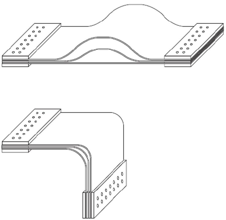
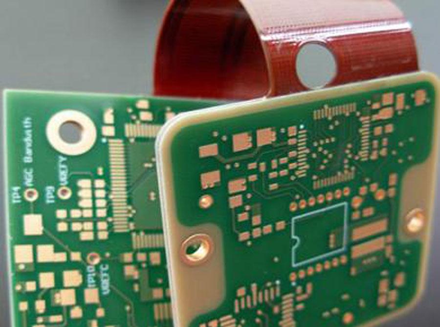
3. Bending and Bending Radius
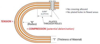
Rule of thumb for calculating the Rigid flex PCB bending radius:
- 1-Layer, Rigid-Flex PCB: = r(min) = 6 x T
- 2-Layer, Rigid-Flex PCB: = r(min) = 10 x T
- Multilayer, Rigid-Flex PCB: = r(min) = (10-15) x T
- Strong dynamic loaded rigid-flex PCB: = r(min) = 25 x T
“T” is the thickness of the flexible PCB
Calculate 150µm for a 1-layer, and 200µm for a 2-layer printed circuit board. It guarantees are already included.
Example: A 2-Layer rigid-flex PCB is 200 microns thick. From the formula above: 10 x 200 microns = 2000μm = 2mm.
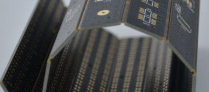
4. Bookbinder bending:
Differential Lengths (Multilayer and Rigid Flex)
The bookbinder design of an unbonded flex area can be used in regions where a sharp bend (radius to thickness ratios < 6) is required. This technique uses progressive lengths in the flex pcb area and is costly to manufacture because of tooling complexity, processing difficulties, and reduced yields.
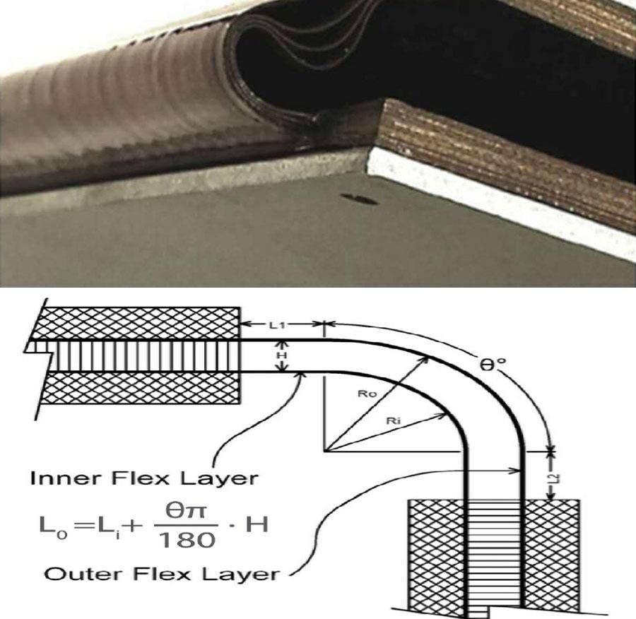
To work out the additional length needed for each flexible circuit layer above the innermost layer, use the calculation given by IPC-2223:
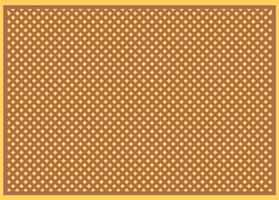
5. Flex Plane Patterns
Solid Copper
-
Least flexible, most effective shielding & impedance reference
Cross-Hatch
-
More flexible than solid copper planes
-
Potential EMI leakage (hatch pitch dependent)
Very common in the field of flex and rigid-flex pcb design is the use of hatched plan layers.
Hatched plan layers increasing the flexibility of Flex and ridged flex PCBs.
6. Flexible PCB constraints areas
Each area in a rigid flexible circuit has its constraints; the mechanical designer shall give description details depending on the final requirements.

It is most cost effective to build a rigid-flex pcb with an even number of layers. All rigid portions of the circuit should have the same number and stack-up of layers.
Hemeixinpcb manufactures single, double, and multi-layer flex circuits using modern rigid-flex materials and stack up. Designs comply with IPC 2223C standards, which define the elimination/minimization of adhesive use within rigid areas, use of adhesiveless based substrates, and use of selective/partial coverlay stack up.
Concept to finish or problem specific, design engineers are available to assist our customers. Contact Hemeixinpcb to begin working with the design engineer most able to help you with your specific design needs. Please send your email to This email address is being protected from spambots. You need JavaScript enabled to view it. if you want to get some help.


