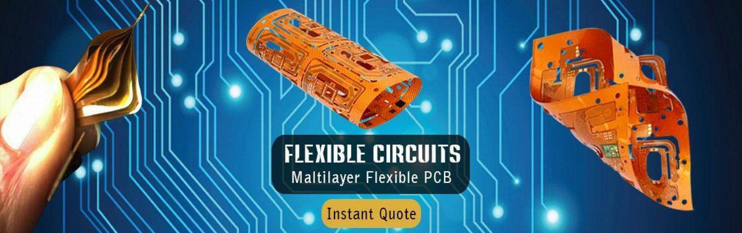
Microwave PCB and High Frequency PCB
What is high frequency pcb
As complexity of electronic components increases, the one thing that becomes imperative is signal rates and high frequency of transmission. Little surprise then that the demand for high frequency PCBs is on the rise. They find use in a variety of high-speed design applications that require a frequency range of 500MHz to 2GHz.
FR-4, based on epoxy resin and glass reinforcement, is the most popular laminate material for printed circuit board industry for a long time. The FR4 dielectric constant ranges from 3.8 to 4.8, depending on the glass weave style, thickness, resin content, and copper foil roughness. However, PCB industry also use other material for different application. In RF/microwave products, low loss and special controlled dielectric constant material like PTFE (Teflon) was widely used. These material was developed long time ago. Partly because of low volume in production, it is quite expensive in the past. When wireless became popular in consumer products years ago, the demand for low loss material was went high. But the material cost is still high. Even some new developed material were trying to get involved, it seems none of them can reduce the material cost dramatically. How to reduce the RF PCB cost became an essential problem for the designer. One of the solution is the mixed dielectric design.
Because the low loss material is not needed for all wireless system, it mostly designed-in, from my understanding, for the circuits from antenna to power amplifier. To reduce the PCB cost, designer used multiple PCB and only the front end of the receiver subsystem need high cost low loss material. However, the cost is still high because of multiple PCB’s and the connector between them. Beside, the Teflon PCB is soft and is comparably difficult in assembly due to warpage.
Mixed dielectric PCB cosist of different dielectric material in on multilayer construction. For example, it can be a 6 layer board with layer 1 to 2 made by Teflon and the rest of layers made by FR-4. There is cost anvantage by using one PCB instead of two or more. No connector is needed and the product dimension can be shrunk. The electrical performance can be improved also for no connector used and signal path is closer together. For assembly work, the mixed dielectric multilayer board is much stiff and easier to manufacture.
Benefits Of Benefits Of High Frequency PCB
- First up, the benefit that high frequency PCBs offer is that they have high density and improved signals. It offers a frequency range of 500MHz - 2GHz, making it ideal for suited for high-speed designs.
- The use of ground plane further enhances the quality of signals as also reduces electromagnetic waves.
- They work well in reducing circuit impedance and provide a shielding effect
- With the reduced distance between plane and trace layer, crosstalk is avoided
- With careful determination of the length and trace width of the board, excessive heating is prevented even at high frequencies.
Microwave PCB and High Frequency PCB–Common Problems and Solutions
RF circuit boards, and Microwave PCBs, are especially difficult to design compared to traditional PCB layouts. This is due to the problems that could arise in receiving or transmitting the radio signals. Some of the main problems are noise sensitivity, and tighter impedance tolerances
Compared to traditional circuit boards, radio and microwave signals are very sensitive to noise and also require much tighter impedance tolerances. The best solution for these problems is to utilize ground plans and use a generous bend radius on impedance controlled traces. These solutions will ultimately allow the RF/Microwave PCB to achieve the best performance.
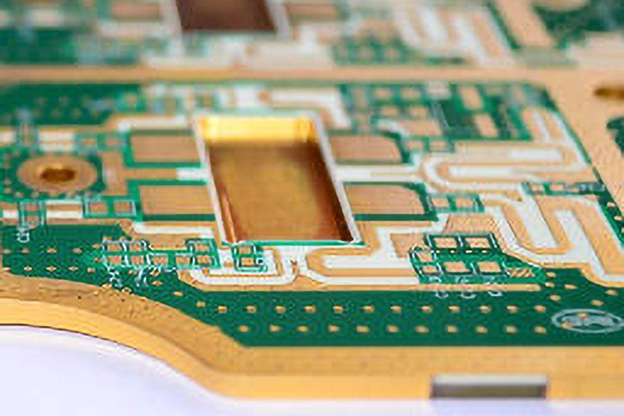
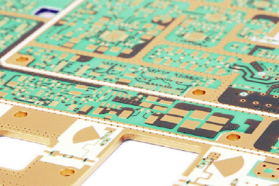
The manufacture of mixed dielectric Hemeixin has been quite standard for many PCB fabricator. The difficulties in manufacturing is to get an optimum production parameter for two or more different materials. Since most of the design are not balanced in construction, the warpage problem need to be carefully managed. It relates to material choice and design as well as the lamination process. Sometimes, use the exotic material on the bottom layer to balance the design can be a solution. But usually it’s not necessary and only bring a lot of cost.
To meet electrical perormance, the mixed dielectric multilayer is deisgned with blind/buried via quite frequently. In some case, it can bond with metal and used in the power amplifier application.
The application for the mixed dielectric Hemeixin is not only for high frequency products. For high speed digital design, it may also help. For example, if there are some critical transmission lines need to pass long distance in PCB and the Df (dissipation factor) of FR-4 material is too high and cause signal integration problem, use some low loss material in part of the inner layer may have great help. It can save some cost instead of using low loss PCB material in all layers.
MEGTRON 6 High Speed, Low Loss Multi-layer Materials
MEGTRON 6/6G is advanced material designed for high-speed network equipment, mainframes, IC testers and high frequency measuring instruments. The main attributes of MEGTRON 6/6G are: low dielectric constant and dielectric dissipation factors, low transmission loss and high heat resistance; Td = 410°C (770°F). MEGTRON 6/6G meets IPC specification 4101 /102 /91.
R-5775 MEGTRON 6 Features
MEGTRON 6 provides excellent high-density interconnect (HDI) and thermal performance.
Ultra-low Loss, Highly Heat Resistant Circuit Board Materials
Low Dielectric Constant (Dk) Glass Cloth - LaminateR-5775(N)/PrepregR-5670(N)
Standard E Glass Cloth - LaminateR-5775/PrepregR-5670
The MEGTRON 6 Family, including MEGTRON 6(G), MEGTRON 6(K), MEGTRON 6(N), are the original PCB industry standards. The products are ideal for mobile, networking, and wireless applications requiring high-speed, ultra-low loss circuit materials.
- Low Dk = 3.7, Low Df = 0.002 (@ 1GHz)
- Excellent through-hole reliability (5x better than our conventional high Tg FR4 material)
- Lead-free, ROHS-compliant soldering
- High heat resistance
What is High Speed PCB Design base on MEGTRON 6 PCB Materials
Select a dielectric material with the lowest loss tangent and smaller dielectric constant, for example, the Megtron6 (df<0.002, epsr=3.1) is an appropriate choice.
- When they become available after vendor characterization, dielectric materials such as Megtron 6N/6G or Tachyan 100G are good selections.
- 25+G designs require special attention to material details including Fiberglass, Dielectric Matrix and Copper. The signal at higher data rate has higher frequency element and the wavelength goes on reducing. The change of fiber glass pattern, dielectric matrix pattern and copper pattern should be considered carefully. As for higher data rate (shorter signal wavelength), it appears to create more discontinuities and reflection with slight change. Please refer to PCB Dielectric Material Selection and Fiber Weave Effect on High-Speed Channel Routing for more information.
Select smaller dielectric height for high speed signal routing.
- It requires smaller trace width for trace impedance target. There is always a trade off between selecting wider trace width and shorter trace width. The wider width has less skin depth and lower insertion loss but takes more space for routing.
- It also results in a smaller PCB height as well as smaller transition via height for achieving minimum impedance mismatching.
Select enough stripline layers for all critical high speed signal routing.
- Hemeixinpcb recommends stripline routing for all critical high speed signals (above 15 Gbps).
- You can route all non-critical high speed signals (below 15 Gbps) on a microstrip layer.
- Stripline routing has maximum isolation with other layers as long as both sides are reference planes. Hemeixinpcb does not recommend dual stripline routing unless the signal routing on both stripline layers are perpendicular. This means, longitudinal broadside coupling of differential pairs should be avoided.
- Hemeixinpcb recommends Stripline preferred over microstrip. If microstrip routing is selected, Hemeixinpcb recommends removing the solder mask.
- Stripline routing requires smaller trace width, which results in more space for signal routing.
Selection of a ground/signal/ground stackup combination for critical high speed signals.
- Selection of a ground/signal/ground combination may be feasible as long as the signal routing crossings on both stripline layers are perpendicular to minimize broadside coupling which results in cross-talk.
Select enough power/GND layers to cover the power supply rails.
MEGTRON 6 Manufacturer
Hemeixinpcb qualified the Panasonic Megtron 6 raw material for its next generation PCB’s while initiating successfully the supply of PCB’s based on Megtron 6 to our valued customers.
Megtron 6 is a new generation, advanced material designed for high frequency (Low Dk, low Df) circuit board applications. Megtron 6’s electrical properties are competitive with PTFE–based materials.
Megtron 6 provides designers significant benefits in system performance for telecommunication applications that demands high-speed Data transfer and computing applications.
High production yield along with positive feedbacks has been received hence the Megtron 6 answers the demands of:
- Advanced material designed for high-speed network equipment, mainframes, IC testers and high frequency measuring instruments.
- The Megtron 6 meets the industry standard for High Speed, Ultra Low Loss Multi-layer Materials
- Megtron 6 meets IPC specification 4101 /102 /91.
- Major applications for Megtron 6 are:
- Networks
- Wireless
- Antennas
- The main attributes of MEGTRON 6 are:
- Low dielectric constant and dielectric dissipation factors.
- Low transmission loss and high heat resistance.
- Excellent through-hole reliability (5x better than conventional high Tg FR4 material).
- Lead-free, ROHS-compliant soldering.
- High heat resistance.
- Excellent HDI and thermal performance.
We have a significant amount of stock in all of the high-frequency laminates as we have been producing PCBs with these materials for many years. Some of the applications of these PCBs are RF antenna, wi-fi (Carrier-Grade and Licensed Access), IP infrastructure, power amplifiers, diplexers/multiplexers, test and measurement, and many more.
With PCBs made from these products, it is important to have significant experience in producing PCBs with these materials, but also you must have invested in the equipment to properly process these RF PCBs. Experience in engineering and CAM is critical to being able to ensure that your PCBs are built to last as these materials all have very different scaling factors along with the fact that they all behave differently; you are removing the copper during the etching process. Without a proper process for managing registration, lamination layer shirt, and other factors using the proper equipment like X-ray, PCB fabricators will have a difficult time producing the yield that gives the customer confidence.
Here at Hemeixinpcb, we work with our customers during the design stage as well as investing in the leading-edge equipment every year to ensure that we stay ahead of the needs for RF PCBs.


