
Controlled Impedance PCB
Owing to significantly increasing transmission frequencies, i.e. shorter pulse rise times of electronic components, in high frequency technology, it has become necessary to treat the conductors concerned as a component. Depending upon a number of parameters, HF signals are reflected on circuit boards. This means that the characteristic impedance differs from the output impedance of the transmitting component. The proper transmission of the signal is thus no longer guaranteed.
A microvia is formed, not drilled like a traditional via. Engineers currently use several processes to produce microvias. Laser drilling, the most common technique, employs a focused laser beam to form the hole. Wet/dry etching is a mass-production process that creates all vias at the same time, regardless of the number or diameter of the holes. Photo imaging coats the base substrate with a dielectric layer. Engineers can also use conductive ink in microvia formation. In such a process, you form the microvias by laser drilling, photo imaging, or insulation displacement. You can also form microvias mechanically, using piercing, punching, abrasive blasting, or simple drilling. Each process produces different microvia hole shapes, such as cups, positive tapers, negative tapers, and straight walls (See below picture).
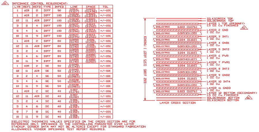
After making the circuit board, the impedances are checked and recorded. The results of the measurements are available on request at any time.
Impedances on the circuit board
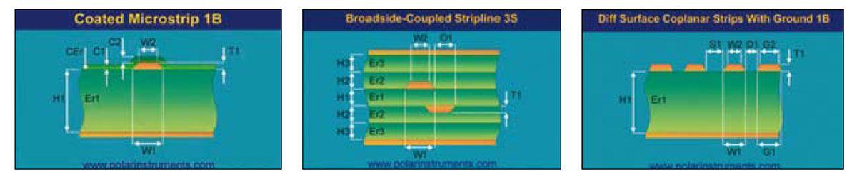
The microstrip is a very simple yet useful way to create a transmission line with a PCB. There are some advantages to using a microstrip transmission line over other alternatives. Modeling approximation can be used to design the microstrip trace. By understanding the microstrip transmission line, designers can properly build these structures to meet their needs.
The impedance specified by the customer will be checked during the PCB maker’s preparatory work to see if it can be made. Depending on the definition of the layers in the stack and on the layout itself, from a set of 93 different models, the correct one must be selected to be able to calculate the impedance. As a result of this, a layer structure will be produced together with any necessary modifications to the geometry of the relevant tracks. The standard tolerance used for an impedance is ±10%. Depending upon various PCB characteristics, on request an improved tolerance (down to ±5%) can be offered.
Typical models for calculations
To be able to actually reach the calculated impedances in the printed circuit board, the manufacturer must understand their production processes very well and have good control of them. The angle of the track edges (resulting from W1, W2 and T1), the pressed thickness depending on the copper coating (H), the thickness of the solder resist varnish (C1, C2) and more, all influence the impedances on the circuit board. The tolerance range of all processes have to be considered here. These values are then added to the formulae for the calculation.
Depending on the complexity of the circuit board, some of the impedances of the circuit board can be checked during the manufacturing process. For this, new models for the corresponding situation (actual state of the circuit board) are separately defined and the results determined.

Dielectrics
To make controlled impedance circuit boards, differing materials are used. FR4 is standard here too. However, in applications with very high frequencies (>1 GHz), requirements such as low dielectric loss or a lower Er are of increasing importance.
Impedance Control: How to Specify Your Requirements for PCB Manufacturers
Give Your Fabricator a Stackup Table
If you’ve created a complete stackup table, then you can include your impedance control spec as a note for your PCB manufacturer. You will typically want to include the following information:
- Trace width you’ve determined for a required single-ended impedance
- Repeat #1 for differential impedance
- Repeat #1 and #2 for each layer
- Specify these values for each transmission line geometry on each layer (coplanar vs. microstrip/stripline)
These points are important to specify clearly as different trace geometries may be present on different layers, and they might also have different impedance values. It’s important to be complete and clear in your PCB fabrication notes. Determination of all the trace widths required to reach impedance targets is one of the essential parts of front-end engineering that should normally be performed by designers. Using the right stackup calculator with anintegrated field solver makes this easy.
Specify Impedance in Your Fab Notes
This is what designers will often do when they only care about impedance matching, but they are not designing the board around their manufacturer’s material stocks. FR4-grade laminates and other materials can be substituted for each other, but this could require changes to the trace widths in your design in order to hit impedance goals. Typically, a designer will choose a material that conforms to a specific slash sheet, and that probably has a specific thermal property they care about. They will then use that dielectric constant to determine the trace width required for a specific impedance.
The impedance will then be specified using a note in a PCB fabrication drawing.
IMPEDANCE REQUIREMENTS:
- ??? OHM IMPEDANCE REQUIRED FOR X.XXX MIL TRACES ON LAYERS X, Y, Z.
- ??? OHM DIFFERENTIAL IMPEDANCE REQUIRED ON X.XXX MIL TRACES / X.XXX MIL SPACING ON LAYERS X, Y, Z.
This is fine as long as you know your fabricator can substitute alternative materials that will ensure the impedance in every layer can hit your targets. This is yet another reason to talk to your fabricator early; ask them for their standard stackups and design rules, and you’ll eliminate the need for design changes later.
Make an Impedance Table
One option is to place a small table in your fabrication drawing that summarizes all the impedance requirements on each layer. Again, you’re only specifying a single width and impedance value on that particular layer. This is either the impedance you determined from a stackup calculator, or it’s the impedance goal you need the fabricator to hit in your design. A simple (color) impedance table you can place in your fab notes is shown below.
Here, HemeixinPCB can offer a large portfolio of usable materials. Many of these are seen as standard and are regularly used, others are available at short notice. You will ἀnd further information in the “Materials”.
Quality control


