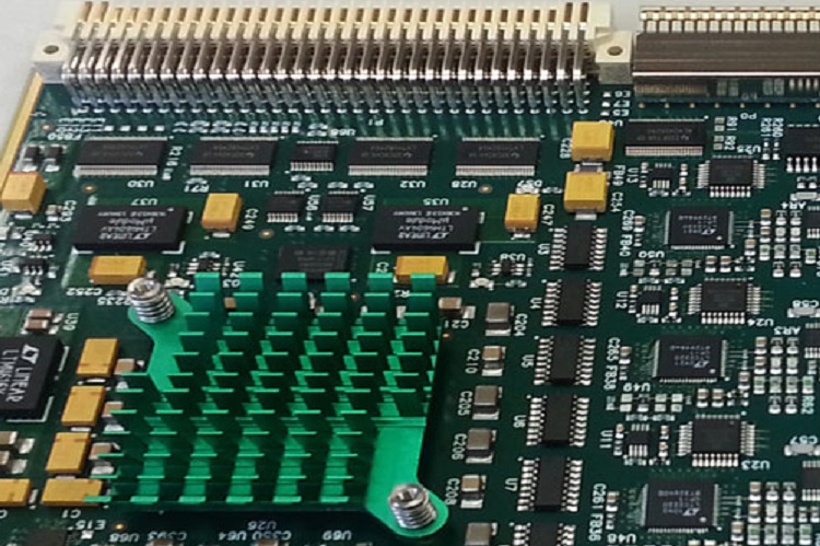
PCB Assembly
 PCB Assembly and printed circuit board assembly Manufacturing
 PCB Assembly and printed circuit board assembly Manufacturing
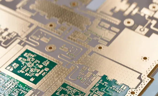
The first stage of the PCB assembly process is applying the solder paste onto the PCB surface. The primary goal is to fill the holes with the appropriate amount of solder paste so that electrical components can be attached later. The solder layer must end up in apertures, while the flat PCB surface should remain intact. Therefore, applying a highly selective technique is mandatory to fill holes of various sizes with appropriate film thickness. One of the most widely used techniques is solder paste printing, representing a standardly used technique in our production plant.
PCB assembly file requirements
Please include the following files with your order. Please include then in a single ZIP file.
- Gerber Files
Please include all the layers (copper, soldermask, silkscreen, solder paste, etc. - Centroid File
Also known as pick and place file. It should include component locations, rotations and reference designators. - Bill of Materials (BOM) in Excel format. Your BOM should include:
- Reference designators
- Quantity of each part
- Manufacturer part number
- Part description
- Type (SMT, Thru-Hole, Fine-pitch, BGA, etc.).
- Package description (QFN32, SOIC, 0805, etc. package is very helpful but not required).
PCB assembly component/ Part guidelines
Guideline for Ordering Board Level Components (Parts) Including Overages
- Extra parts will be required on small builds (1 to 25 boards) to be as follow:
- 0201 to 0603 size: Minimum extra quantity 25 plus required quantity
- 0805 to 1206 size: Minimum extra quantity 10 plus required quantity
- On large size components 1 or 2 extra parts is fine
- All items must be on a continuous strip or reel
- For large runs extra parts by percentage is OK
- Special instructions must be provided if components need special handling such as no clean solder.
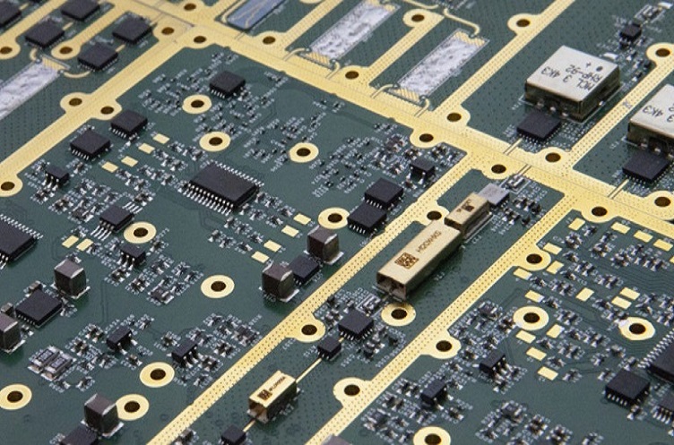
PCB assembly capabilities overview
- BGA, micro-BGA, QFN, CSP and any leadless devices up to .20mm pitch assembly with 100% 3D X-ray inspection
- PCB components, including all types of BGAs, QFNs, CSPs, 0201, 01005, 08004, POP, and press fit components in small quantities
- DFA process identifies almost all manufacturing issues before actual assembly saving production holdups
- RoHS, leaded, indium, clean & no clean chemistries
- Paste in-hole
- De-ionized water cleaning of assembled boards
| PCB Assembly Capabilities | |
| Lead Time | 2 - 5 Days, 1 - 2 Weeks and Scheduled Deliveries |
| Parts Procurement | Full Turnkey, Partial Turnkey and Kitted/Consigned |
| Assembly Types | Surface Mount (SMT), Thru-hole, Mixed Technology (SMT/Thru-hole), Single and Double Sided SMT/PTH, Large Parts on Both Sides, BGA on Both Sides |
| Board Type | Rigid Boards, Flex Boards and Rigid-Flex Boards |
| Stencils | Laser Cut Stainless Steel and Nano-coating |
| Components | Passive Components Smallest Size 01005, Fine Pitch Components Smallest Size 8 Mils Pitch, Leadless Chip Carriers/BGA, VFBGA, FPGA & DFN, Connectors and Terminals |
| Largest PCB Size | 18'' x 20'' |
| Smallest PCB Size | 1.2'' wide |
| Largest QFP Size | 75 mm x 75 mm |
| BGA Pitch Range | From 0.20 mm to 3 mm |
| Smallest QFP Pitch Range | From 0.20 mm to 3 mm |
| Component packaging | Reels, Cut tape, Tube and Loose Parts |
| Inspection | X-ray Analysis, AOI and Microscope to 20X |
| Solder Type | Leaded and Lead-free/RoHS Compliant |
| Assembly surface mount connectors | Yes |
| Wave Soldering | Yes |
| PCB Finish | SMOBC/HASL, Electrolytic Gold, Electroless Gold, Electroless Silver, Immersion Gold, Immersion Tin and OSP |
| Panelized PCB | Tab Routed, Breakaway Tabs, V-Scored and Routed + V-scored |
| Design File Format | Gerber RS-274X, Eagle and AutoCAD’s DXF, DWG BOM (Bill of Materials) and Pick and Place file (XYRS) |
Full turnkey PCBs
Hemeixin creates an unbroken thread from design to delivery. Receive a complete quote for fabrication, assembly, and components—entirely online. Our white-glove service brings your product to life.
Partially consigned assembly
Some parts provided by the designer — we will source the rest. Hemeixin will work with your supply chain to get your PCBs assembled and to market quickly.
Consigned assembly
All components are provided by the PCB designer. Hemeixin will fully assemble your PCBs and ship them to you. Quick turn times available, with fully transparent pricing.
PCB assembly process overview
- Our team confirms the necessary files and order details.
- Manufacture SMT stencil (if needed).
- Program our machines from the BOM and Centroid file, before the materials arrive. Discrepancies found in the files will be addressed.
- After all the materials are received, our team performs a kit audit of the materials. Discrepancies or additional questions will be addressed. Before the assembly lead time begins we must have all questions answered
- If all materials are in before 12pm PST, the assembly lead time starts the next business day. Materials received after 12pm PST will be considered received on the next business day.The reason for this is to allow proper time for the materials to go through the kit audit process.
- The SMT components are assembled first with our automated equipment. The first board goes through extensive QA to assure part placement and polarity are correct. The boards are then inspected (visually and with an AOI machine) as they come off the reflow oven.
- BGA components are X-rayed to verify placement accuracy and to detect any solder bridges.
- After SMT the boards are washed when applicable.
- Thru-hole components are inserted and soldered by hand or with a selective soldering machine depending on the quantity and board design.
- After thru-hole boards are washed again when applicable.
- A final quality inspection is performed.
- The finished PC board assemblies and all extra materials are prepped for packaging. Your materials are shipped back to you, tracking number is sent via email
PCB assembly service checklist
Hemeixin wants our customers to experience a seamless and accurate assembly process. To ensure that your job is not placed on hold, please follow these guidelines:
- Accurate Data
An error free assembly process requires accurate data. Each job should have a BOM (bill of materials), a pick and place file (also known as a centroid file) and matching Gerber data. Add a DO NOT POPULATE (DNP) column to the BOM if there are parts which should not be populated on the PCB. - Ensure Proper Footprints
Some parts are available in different packages. Make sure that the part you specify in the BOM matches the footprint on the PCB. - Organize Components
Parts should be separated into individual bags or trays. Each bag or tray should be marked with Manufacturer name and Manufacturer part number and all reference designators where the part is used. If needed, you can substitute distributor name and part number in place of (or in addition to) manufacturer information. - Multiple Jobs Per Order
The parts for each job should be packaged separately. Include separate BOM and pick and place file for each job - Component Quantities
Include extra parts to account for possible attrition during assembly.
Extra parts will be required on small builds (1 to 25 boards) as follows:
- 0201 to 0603 size: Minimum extra quantity 50 plus required quantity.
- 0805 to 1206 size: Minimum extra quantity 25 plus required quantity.
- On large size components 1 or 2 extra parts is fine.
- We prefer all SMT parts to be on a continuous strip or reel.
- For large runs extra parts by percentage is OK
We will return any unused parts to you when we ship your assembled boards back to you.
- Update your BOM and Pick and Place File
If you have any last-minute design changes, please remember to reflect these changes in your BOM, pick and place file and any other relevant documentation. - Mark Polarity
Make sure you indicate proper orientation for all parts that have polarity. Place a dot or a number “1” on pin 1 of ICs where the orientation is not obvious. Ensure that polarized capacitors and diodes are properly marked. - Special Instructions
Provide detailed instructions for any special procedures required to assemble your boards. Include sketches, photos, PDF files and/or drawings as needed - Drop Shipping from Suppliers
Please ask your suppliers to place your PCB Hemeixin Order Number on the outside of any package dropped shipped to us.
PCB assembly process
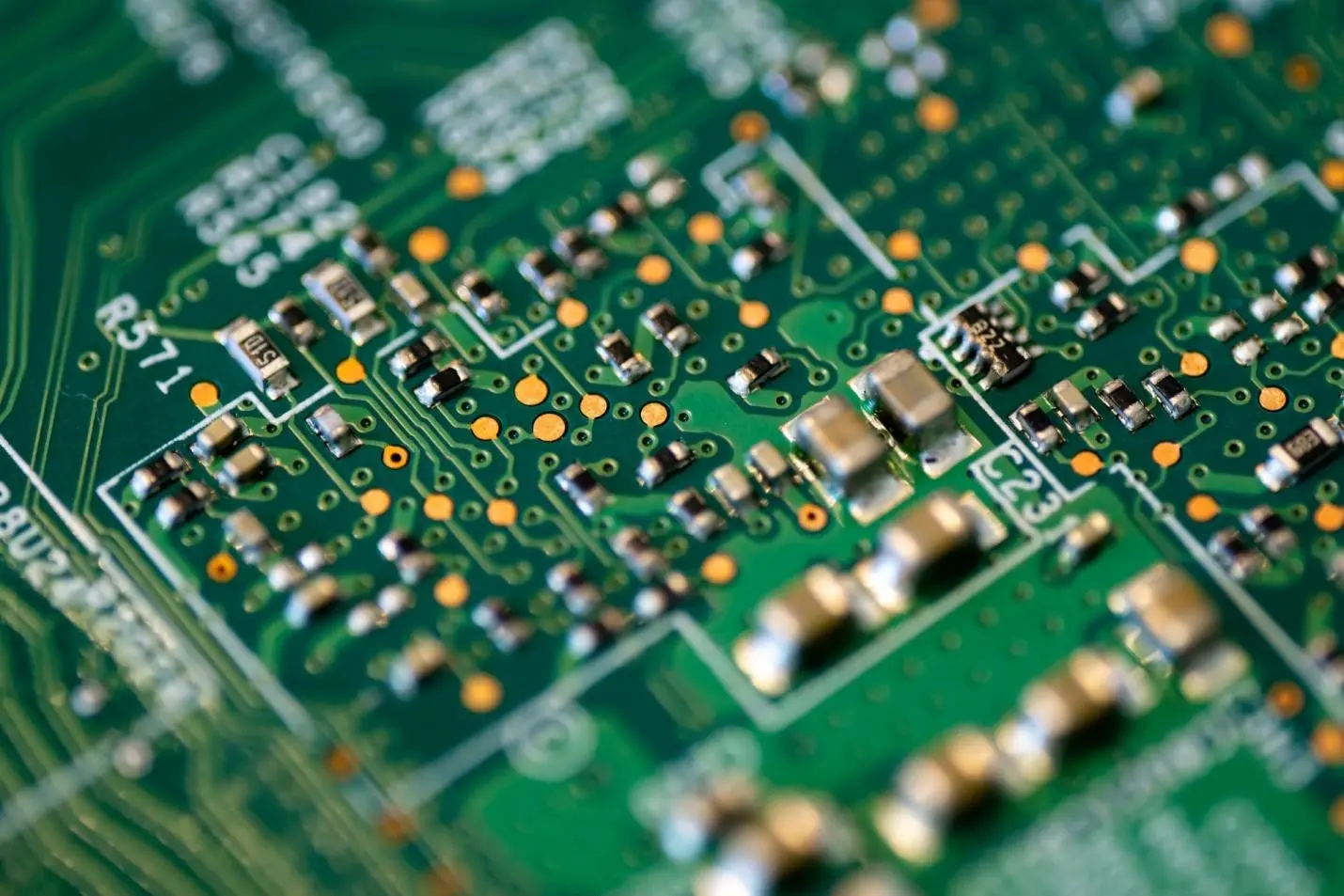
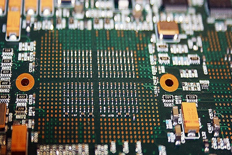
The PCB assembly process occurs after PCB manufacturing, where the board structure is completely formed according to client requirements. The PCB assembly covers actions from stencil preparation and solder paste printing to SMD parts placement, bonds formation in the curing oven, and final inspection of the PCB functionality. After stencil preparation, the solder paste printing takes place. At this stage, tiny apertures that present mounting spots for electrical components must be filled with exceptional precision. Otherwise, some serious issues such as bridging may occur. The bridges often have a micro size and are not visible to the bare eye. That makes them hardly detectable if state-of-the-art inspection devices are not used. Still, they are the most common issue in the PCB assembly process, leading to short circuits or even component burning up. Thus, we at Semecs utilize the latest solder paste printing technology, ensuring that every single printed circuit board operates appropriately at the end of the assembly line.
Another critical part of the PCB assembly process is the positioning of electronic components using the pick and place machine. The conductive lines at the board are very tiny, and they must be aligned with the conductive parts of the electronic components. Hence, the electronic devices must be orientated and posted on the board with the highest precision. We use the most precise three fiducial points optical systems to place the surface mounting devices. Finally, at the end of the PCB assembly line, the firm and stable connection between SMDs and board is achieved in the curing oven. The paste soldering enables the PCBs' longevity and durability, which are our ultimate goals besides the PCBs' highest quality.
PCB assembly is a guided, step-by-step process. The first step in the process is stenciling, where solder paste is applied to the sections of the board where components will be mounted. Solder paste is made up of microscopic metal balls and a substance called flux. Solder paste stenciling is like screen-printing; solder paste is applied to the bare PCB using a thin stainless steel stencil. A mechanical fixture holds the stencil and the PCB in place while solder paste is distributed over the stencil. The paste is viscous and will remain in the specified areas of the bare PCB after the stencil and applicator are removed.
Stencil preparation
The metal sheet should cover the entire surface of the print circuit board except for the holes filled with the solder paste later on. Therefore, the metal sheet must be processed to follow the PCB pattern defined by industrial design, where apertures within the sheet have the same shape, width, and length as their pair holes at the PCB. This metal sheet is widely called a stencil, made of whether brass or stainless steel.
The stencil design is a highly challenging task since the precision of the stencil's shape and uniformity of stencil thickness are essential for accurate and purposeful PCB assembly. The typical thickness range of a stencil is between 0.0254mm and 0.762mm. The metal sheet thickness is a parameter that depends on the types of electric components used in the particular PCB, and it is determined separately for each printed circuit board. Even the slightest under or oversizing may cause significant issues in later stages of the PCB assembly process. The larger stencil apertures cause so-called balling or bridging. Those phenomena arise during solder application where film covers parts of PCB surface or even whole pathway between two neighbor holes. The result of both cases is an open electric circuit that leaves PCB completely unfunctional. After selecting the required stencil parameters, the metal sheet with specified composition and thickness is ordered from the metal factory, which inspects the sheet's thickness uniformity using x rays gauge and then ships it to our production plant.
Chemical etching
There are few stencil processing technologies, but laser cutting and chemical etching are the most widely used ones. In the chemical etching process, the metal mask and flexible metal mask are etched from both sides. Firstly, the PCB design should be transferred onto the metal sheet using film. Then, sheets are dipped into the specific acid solution, which enables aperture formation. However, the drawback of this process is that acid interferes with deeper sheet levels, causing undercutting. Therefore, the walls must be additionally polished to form a smooth surface suitable for solder application during PCB assembly. There are two options for wall smoothening: electropolishing which presents a micro etching process, and nickel plating. Electropolishing is a reverse process of electroplating. The electricity is utilized to dissolve excessive metal parts into an electrolyte solution which is swept after processing. Conversely, during the nickel plating, the additional metal layer is applied to walls of apertures whose diameters consequently become reduced.
Laser cutting PCB
Specialized CNC machines are used for laser cutting PCB purposes during the PCB assembly process. Applied laser beams cut the metal sheet according to the pattern provided by the Gerber file. This file contains all technical specifications of PCB, while integrated custom software reads them and then navigates the laser moves through the cutting process accordingly. Since the metallic bond is outstandingly strong, the fine-tunning of laser parameters is necessary to create smooth metal edges. The following parameters play a crucial role during the laser cutting PCB process: beam spot size, beam focus, cutting speed, and laser power. The laser power must be sufficient at all times to enable rays' penetration through the sheet surface. A beam spot of 0.0254mm is the most widely used one in the PCB assembly since it is suitable for cutting almost all kinds of shapes and aperture sizes. Regardless of the set parameters' accuracy, there is a need for additional smoothing of aperture walls using the same techniques as in the chemical etching process, either electropolishing or nickel plating.
Solder paste printing
The unique printer kind is used for solder paste applications during the PCB assembly process. This type of printer is widely called a squeegee blade printer. It got its name from squeegees used to press the solder paste across the stencil surface and inside the PCB holes. They may be made either from metal or polyurethane, depending on the pressure ranges they need to generate. The printer's internal vision system aligns the stencil vertically over the boards. In addition, the printer uses three fiducials, commonly called global fiducial marks, for the stencil's highest precision positioning over the board. Namely, the global fiducial mark immediately determines and corrects any eventual PCB misalignment in both the X and Y axes before printing operation and during the printing as well. In that way, the possible displacement of either board or stencil under pressure generated by the squeegee is completely avoided.
Squeegee pressure is a parameter that must be controlled with special attention. Increased pressure may cause multiple issues such as greater paste shear that causes paste spreading over the PCB flat surface and causes so-called bridging and bleeding of solder paste. Since the paste is a highly viscous suspension, it requires significant force to flow. The squeegee pressure must be sufficient to generate the force that overcomes the high friction force between the highly viscous paste and the stencil. Once paste movement is initiated, the paste travels across the width of the printable area in a controlled roll, filling in all stencil apertures while simultaneously being swept from the top side of the stencil surface by squeegee blades. The standard operating pressure range of the squeegee is between 0.13kg and 0.27kg per linear centimeter of the printable area. The moving squeegee must induce inertia under whose influence the paste flows inside the PCB holes. Abrupt but controlled motions of squeegees induce inertia, which is why the speed is another parameter that must be monitored continuously. Since the squeegee's pressure and speed are directly proportional, the speed must be continuously below the upper constraint value, usually 75mm per second. The higher speeds induce the higher friction force between the blades and stencil, leading to blades' mechanical failure over time.
The third essential parameter of solder printing is the angle between the squeegees and the stencil. The regularly set angle is 60° for the following reason. It forms an optimal incline, so the paste moves downwards to the PCB holes by gravity. If the angle increases, it can cause scooping of the holder paste out of the stencil apertures and consequently an insufficient amount of solder paste. On the contrary, the blades leave a solder paste residue on the stencil after the squeegee has completed a print when the angle decreases.
A regular printing operation lasts between 15 to 45 seconds per print circuit board. The printing is the longest step in PCB assembly, followed by the separation process in which the stencil is separated from the PCB. Postprint inspection is essential for quality assurance of deposited solder paste layers and their suitability for the following step-surface mounting of electrical components. The quality assurance is usually performed with unique 2D vision systems on the printer or separate 3D systems.
Stencil separation and cleaning
The PCB is separated from the stencil at the end of the printing process. During separation, the solder paste must remain in the PCB holes. The speed of stencil removal is crucial to ensure that the stencil doesn't withdraw any paste from apertures. The regular linear speed of stencil movement is around 3mm per second. The solder paste can't fully release from the apertures at higher speeds, causing undesired high edges around the deposits.
After few printing operations, the stencil cleaning ensures that there is no accumulation of the paste particles between the stencil and the PCB. The cleaning operation is comprised of two steps: Firstly, the stencil is swept using cleaning chemicals like isopropyl alcohol. In this step, the area underneath the stencil is cleaned. Then, additional vacuum cleaning occurs where the apertures are cleaned to avoid blocking paste flow to PCB holes.
Quality assurance of stencil and squeegee condition after a printing session
Before quality assurance of mechanical parts, the automated cleaning system removes the solder paste residues altogether, so the operator has a clear view of the entire material surface. Then, the operator proceeds with a visual inspection of stencils and squeegees to check if any mechanical defect arose on both blades and stencils. If the operator notices any damage on squeegees or stencils, he needs to replace a defective part to provide a reliable and efficient printing process.
Solder paste composition, properties, and storage
Composition
Solder paste represents a suspension composed of the metal solder particles dispersed in the flux. The metal solders may be made of various elements, but the most common composition is 99.7% tin and 0.3% copper. The metal particles have a spherical shape, and their size may vary according to the type standards specified in IPC J-STD 005. Lead was commonly used in the formulation back in the day. Nowadays, its usage is abandoned due to international environmental protection regulations since it presents a highly hazardous element for human health and the environment. On the other side, the flux is used as an adhesive that bonds the metal spheres and enables electronic components' mounting to pads on the board. The flux is a highly viscous material containing 60 to 80% of active ingredients that hold metal particles together and prevent oxidation and corrosion. The large percentage of active ingredients within flux prevents the formation of metal oxides on both the base and filler materials to which it is applied.
Furthermore, the flux makes it possible to solder through-hole pin in paste components by printing solder paste in the holes. By weight, a mixed solder paste commonly consists of 90% metal. However, due to their lower density, the non-metallic ingredients of the flux take up to one early half of the paste volume.
Properties
Solder paste is a non-Newtonian type of fluid, more precisely the pseudo-plastic one, meaning that its resistance to flow significantly drops after applied pressure reaches a specific value. The pseudo-plastic behavior is an essential characteristic of the solder paste that allows successful printing. Namely, due to significant changes in flow resistance, the paste may flow in and out of the stencil apertures during the print stroke, but it remains in PCB holes without slumping when the print stroke is done.
The viscosity is a physical property that determines the fluid's resistance to flow. Besides the compounds that flux comprises, the greatest influence upon flow resistance has a metal to flux ratio. The increase of the metal compounds significantly increases the overall solder paste viscosity. During the printing operation, the thin solder film between the blade and stencil faces a notable temperature increase that reduces the paste viscosity since it is a consequence of a friction force that arises from applied pressure.
Storage of the solder paste
The appropriate storage of solder paste allows maintenance of its desired properties needed for the highest performance of PCB assembly. The solder paste must be stored in an airtight or hermetic container to prevent metal interaction with oxygen and moisture. The large surface area of sphere-shaped metal particles makes them highly prone to corrosion, which decreases the bonding strength in interaction with electronic components. Another parameter that must be controlled is temperature. The storing temperature should be lower than 8 degrees Celsius, while the 1 degree is the lower temperature limit since flux contain the liquid components that could freeze. The controlled storage conditions reduce the oxidation rate of metal particles, but they also reduce the rate at which the thermosensitive flux active ingredients degrade.
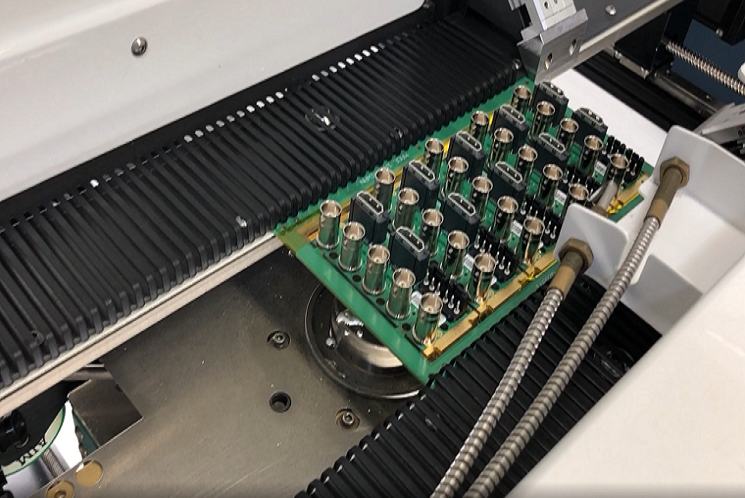
Electrical components' mounting
Once solder paste is applied onto the PCB surface, the mounting of the electrical components is done using a so-called pick and place machine. Before putting the pick and place machine to work, its operation algorithm must be programmed by uploading the bill of materials and component placement list to the Mycronic Mycenter workstation. After programming, the operator supplies pick and place machine with all needed electrical components. Now, this robotic device is ready to begin to operate. During its operation, the accuracy of components placement is the critical parameter that reflects the quality of the PCB assembly process. Like the squeegee blade printer, the pick and place machines use three fiducial points to locate the panel and determine the orientation. The fiducials are optical targets that are etched in the copper layer of every board.
Every component gets its barcode that the machine recognizes while the software sends the information about a particular component position at the board. Besides identifying the component and its place, the device detects its dimension and needed rotation angle for its successful placement. This machine also proceeds with the quality assurance of electrical components since it measures capacitance, resistance, and inductance while carrying it. If the discrepancy between the designed and measured parameters of a particular component is detected, the machine immediately removes that component.
Automated Placement
Component placement is automated using a pick-and-place machine. In the case of through-hole technology, a technician can manually place some components that may be too large for some pick-and-place machines, although at high volume the entire process is generally automated. Fast, accurate, error-free placement with automatic component mounting requires precise numerical data generated from the ECAD data for a design. The pick-and-place file contains each component's X and Y coordinates; this file is generated from CAD software and it is used to program a pick-and-place machine.
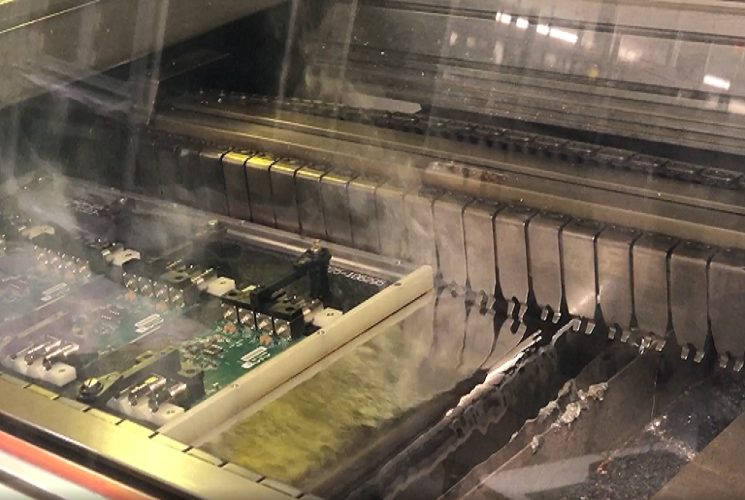
Soldering
Components on the PCB are secured using three possible soldering processes: wave soldering, reflow soldering, and selective soldering. Most boards will only require wave soldering and reflow soldering. Hand soldering is generally not performed in high-volume assembly operations unless rework is being performed.
Wave soldering can be used in both surface mount and through-hole assembly processes, although this will generally be used for through-hole soldering. PCB with all mounted components is moved into a solder line and a hot wave of liquid solder is pulled over the PCB. The solder sticks to the metal portions of the board that aren't covered by solder mask. As the solder cools, it securely fastens component pins to the PCB. Compared to manual soldering, this technique is significantly more efficient and can produce higher quality assemblies.
Reflow soldering is the standard process used for surface-mount assembly. Double-sided boards will pass through two reflow soldering cycles. When used with a hybrid assembly process, this leads to a total of at least three solder cycles (1 wave, 2 reflow, rework cycles) required to fully assemble the PCB. This is an important point to note as some industries require the total number of solder cycles to be limited.
Reflow soldering is completed by placing the components with a pick-and-place machine, and the board is passed into a reflow oven held near 250 Celsius. The oven heats up the solder paste and causes it to harden into a metal joint on the exposed component pins and pads on the PCB.
After the soldering processes are completed, the assembled PCB must be thoroughly cleaned after assembly. This can involve use of deionized water or other cleaning agents to remove any residues from the surface of the PCB, particularly removal of flux residues. After being washed, PCBs are dried with compressed air and the assembled boards are sent for inspection.
Soldering in curing oven
Once placed at the PCB surface, the electrical components must be permanently fixed to it. The permanent fixture is enabled by soldering of the solder paste that firstly melts and then hardens. During hardening, the spatial orientation of atoms within solder changes, and the consequent transition of solder's physical properties induce the solder joints' high tensile strength. The melting process occurs in the curing oven, where PCBs travel through it via a conveyor belt. The heated air flows in the counterflow direction relative to conveyor belt movement. The air with a temperature between 250 and 480 degrees Celsius heats the PCBs via a highly efficient convective heat transfer mechanism. Since paste's set temperature is reached quickly, the curing process lasts shortly, after which the hardening process occurs. The hardening process also happens in the oven, where the atmospheric air cools down the melted solder and finally hardens it.
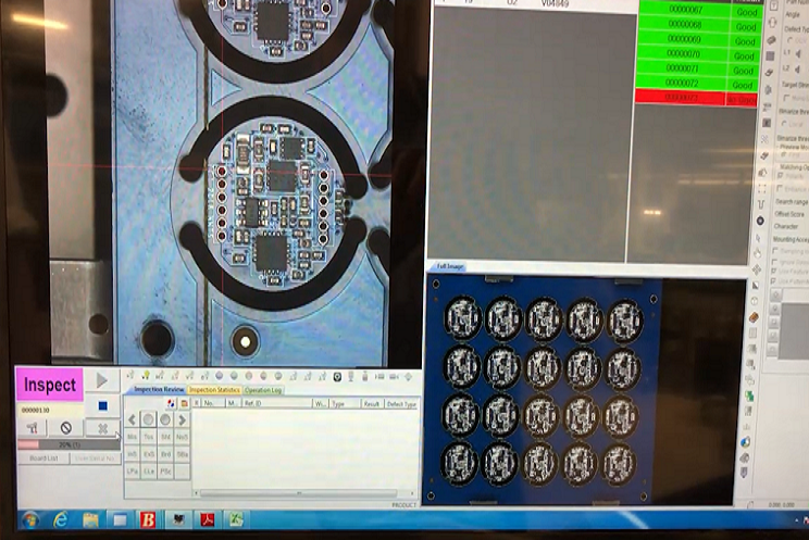
Inspection and functional test
After the PCB assembly process, the operators visually inspect the PCB to check whether all parts are positioned correctly. After visual inspection, the PCB is connected to the power supply for functional testing. During this test, the normal circumstances in which the PCB operates are simulated, and if no defects are detected, the board is ready for shipment.
To make sure that the assembled PCB is in proper working order, the PCB will be inspected with some automated tests. High-volume production will involve further quality assessments to ensure the overall process is producing defects at acceptably low rates. After inspection, some boards may be further qualified with in-circuit testing, which will involve powering up the board and probing specific points on the PCBA.
Visual inspection is performed with automated optical inspection (AOI). This vision system uses high-resolution cameras that can be positioned at various angles to visually inspect the surface layers of the PCBA. The goal in this inspection step is to identify assembly defects related to component placement and soldering. These include component alignment, solder joint quality, and any lifting of components during cooling. Large batches of PCBs can be processed quickly with an AOI system.
For single or double-sized PCBs, AOI will be a comprehensive inspection tool, but it cannot be used to examine inner layers on a multi-layer PCB. Instead, multilayer PCBs can be inspected using an X-ray imaging machine. Experienced technicians can inspect these X-ray images visually, although newer systems can automate the inspection process through some image processing steps. When a defect is found in the X-ray image, it is then flagged for further inspection by a human technician. X-ray systems are also commonly used to inspect BGAs for assembly defects, such as creation of shorts or opens, as well as alignment of the BGA on its pads.
Testing processes for a completed PCBA can vary, depending on the needs of the end product and its required level of reliability. The testing processes used to qualify PCBAs can extend beyond in-circuit testing to include mechanical testing, accelerated life testing, and stress tests like thermal and mechanical shocks. These tests go beyond defect detection and basic functionality checks to determine the long-term reliability of the end product. Depending on the standards that apply to your assembly, different testing regimes may be needed and an industry-focused EMS company should be consulted to develop a test plan.
Our printed circuit board assembly services include:
The PCB assembly process involves mounting and soldering components in three possible process steps:
- Through-hole technology
- Surface-mount technology
- Hybrid assembly
Most modern boards intended for commercial products and advanced technology will be assembled with both surface-mount and through-hole components (hybrid assembly). Most designs will use surface-mount components as they also tend to be smaller, while the larger components like connectors or mechanical parts are still through-hole components.
Advanced electronics do not predominantly use through-hole technology for the major components. However, there are many components that are not central to digital or analog processing that are placed as through-hole components. In this assembly process, the component leads are inserted into pre-drilled holes in the PCB. The leads are then soldered on the opposite side of the circuit board. Through-hole components are typically the bulkiest components on a PCB; some example components include transformers, pin headers, and larger power transistors.
The smallest components used in modern microelectronics are surface-mount devices. These components are directly soldered onto the PCB and they do not require drilled holes for mounting. Note that some connectors will have both drilled hole leads for mechanical stability, as well as SMD pads for surface-mounted connectors. Because drilled holes are not required for these components, the PCB fabrication cost could be reduced in simpler boards and production throughput can be accelerated. Component placement can be almost ten times faster than a typical through-hole placement process, and these components can be placed with far higher levels of component density compared to through-hole components.
It is common to see PCBAs with a combination of surface-mount and through-hole components. When providing a circuit board to a manufacturer for quote, the assembler will need to know if the board will use both through-hole and surface mount components. The issue is that mixing components can add additional soldering cycles because the two types of components require different soldering processes.
Types of PCB Assembly services and Inspection
SMT Assembly
Surface mount technology (SMT) is the most commonly used process in the industry when it comes to Surface Mount (SMT) PCB Assembly. Not without any reason, it allows for components to be mounted directly on the surface mount PCB. The technique lends itself to miniaturization of assemblies, which is the order of the day. Also, SMT Assembly (Surface Mount Assembly) known for their high mechanical strength. The SMT printed circuit boards are a preferred choice for high-speed circuits.
Surface mount technology assembly is a technique in which electrical and electronic components are mounted directly on the surface of a circuit board. Electrical and electronic components that follow this mounting technique are known as surface mount devices (SMD). This technology minimizes fabrication costs and increases efficiency.
At Hemeixin, we have over 15 years of experience in SMT PCB Assembly. With automated SMT Assembly process our boards ensure optimal performance in the most challenging applications.
Hemeixin provides customers with decades of leadership and experience in advanced PCB assembly technology, with proven processes and a full range of services. From prototyping, low volume high mix to high volume global manufacturing, we provide printed circuit board assembly services in China.
Hemeixin is a recognized leader in PCBA and SMT production and develops solutions for our customers using the latest in PCB assembly and surface mount technology. Capabilities include support for:
- 01005 components, fine pitch and high count BGAs, Package on Package (POP), Chip on Board, fiber optics, RF microelectronics, press fit connectors
- Hybrid processes (tin-lead and lead-free), pin through hole, wave & selective soldering, double and single sided reflow, wide body and backplanes
- Quick turn prototype assembly, RoHS compliance certification, conformal & parylene coating, laser marking
- Inspection and testing using the latest SPI, AOI, Flying probe and X-Ray equipment
- Comprehensive electrical testing and test system development for boundary scan, in-circuit test (ICT), functional test and burn in test (BIT)
Prototype pcb assembly
Printed Circuit Board (PCB) prototypes are used to reduce the number of errors or defects in the design of a circuit board at an earlier stage.
Printed Circuit Board (PCB) prototypes are widely used to reduce the number of errors in a PCB design. These prototypes help original equipment manufacturers (OEMs) analyze the strengths and weak areas of their proposed circuits. Prototyping helps manufacturers save on costs that otherwise would be spent on rectifying defects and minimizing product recalls. This is why most companies prefer to invest in a prototype PCB assembly before high-volume production. Partnering with an experienced PCB assembly services provider like Hemeixin Assembly offers several advantages to them. We can handle prototype PCB assembly in quantities from 1 to 100 boards.
Highlights of Hemeixin Assembly’s Prototype PCB Assembly Services
At Hemeixin Assembly, we have acquired capabilities that enable us to serve our clients better. All these years, we have worked on several complex prototype PCB assembly projects, and we believe the following capabilities have helped us serve our clients better.
Printed Circuit Board Engineering Services: We can provide prototype PCB assemblies for design for manufacturability (DFM) and design for testing (DFT). In addition to this we can perform process failure mode effects analysis (PFMEA) and devise control plans.
Prototype PCB Assembly Services: We specialize in the following prototype printed circuit board assembly services.
- SMT: We can provide single-sided and double-sided surface mount PCB assemblies indifferent specifications.
- Plated Through Hole: We offer plated through hole assembly with selective soldering.
- Mixed Assemblies: We often work on projects involving mixed assemblies – through-hole and SMT and electromechanical assemblies.
- In addition to this, we also support new product introduction (NPI) projects.
PCBA Testing: All the PCBA functional testing is performed in-house at our well-equipped facility at China. Over the years, we have invested in various test fixtures and equipment, which helps us ensure the quality of PCBA. Currently, we provide the following types of PCBA testing services:
- Flying probe testing also including boundary testing
- Functional testing including system and board-level testing
General PCB Assembly Capabilities: Our general PCB assembly capabilities are not limited to these:
- RoHS, leaded, clean and no chemistries
- PCB components including various types of QFNs, BGAs, CSPs, POP, 01005, 0201,08004, and press fit components in small quantities
- Paste-in hole
Turnkey PCB Assembly
PCB fabrication with utmost quality is at the heart of Hemeixin Electronics Co., Ltd. We specialize in various types of PCB assembly projects, including full turnkey PCB assembly. With our full turnkey PCB assembly services, we handle all aspects of PCB fabrication. We offer fast, and reliable turnkey PCB assembly as we are experts in procuring components, assembly, testing, delivery, aftermarket service and warranty support.
We’ve worked with small hardware startups and large defense companies, and one thing they tend to need is help navigating the electronics supply chain and manufacturing landscape. If you’re not involved in the industry, PCB manufacturing services can seem opaque and difficult to navigate, just like many other specialized services.
Therefore, it’s often the case that clients will look to a manufacturer that can help guide them through the production process. Turnkey PCB manufacturing services, turnkey PCB assembly services, and contract manufacturing services can help guide you through the process by taking on many of the important management tasks needed to complete a manufacturing run. Sometimes, it makes much more sense to contract these services through your design firm, rather than through a manufacturer. With a single source approach, we can take any complex project, and turn it around in a short lead time, whilst not compromising on the quality. Being a leading form of electronic assembly, turnkey PCB assembly services bring several benefits to the customers as follow.
- Our full turnkey PCB assembly is a highly-efficient and fast form of electronic assembly. You don’t need to worry about managing multiple vendors as we take care of the entire fabrication.
- With our full turnkey PCB assembly services, you can build and refine prototypes faster, easier, and cost-effectively.
- We are all equipped to handle (through-hole, surface mount, mixed) small batch of boards or full production runs.
- We have verified supply chain networks to support the entire process of turnkey assembly. With end-to-end solutions from a single provider, you can gain significant cost savings, too.
- We have a team of highly qualified staff who are experienced in working on turn-key circuit board assembly. They not only help meet your expectation in terms of quality, but also complete your projects faster.
We offer instant quotes for your turnkey PCB assembly order and you don’t need to wait for long to know how much the order would cost. Also, you can see the real-time status of your project. This helps you to monitor the PCB manufacturing stage. With a single point of contact, and flexible services, Hemeixin Assembly’s full turnkey electronics assembly meets the unique needs of small businesses, large corporations, and entrepreneurs.
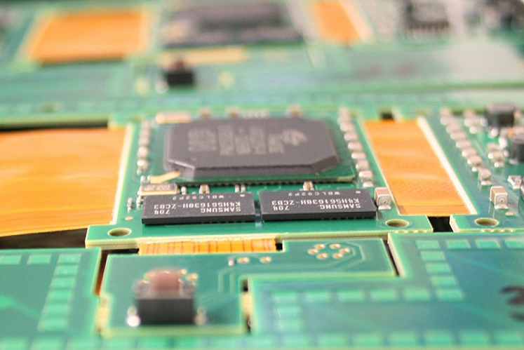
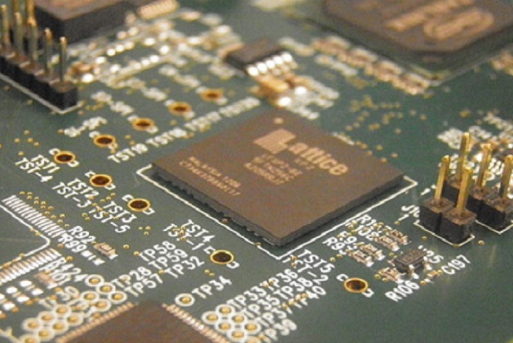
BGA Assembly
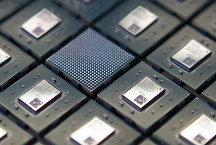
Implementing complex and small-size chips in PCB designs is necessary to match the technological advancements taking place around us. Such ICs increase the packaging I/O density. Thus, high-density and low-cost packaging methods are in great need. BGA is one among them.
BGA assembly is a process of mounting ball grid arrays (BGAs) onto a PCB using the solder reflow process. BGAs are surface mount components that use arrays of solder balls to make electrical interconnections. These solder balls melt and establish interconnection when the board passes through the solder reflow oven.
What are the advantages of a BGA assembly?
- Improves both electrical and thermal performance while making efficient use of space.
- Reduces the overall thickness of the board.
- Minimizes the chances of PCB damage since BGA leads are made from solid solder balls, consequently reducing maintenance and repair times.
- Suitable for miniature packages with high pin count.
- Offers improved solderability, resulting in a speedy assembly procedure.
- Dissipates heat quickly due to low thermal resistance.
BGA (Ball Grid Array) Assembly Services with X-ray Inspection
Hemeixin has been providing BGA assembly, including BGA Rework and BGA Reballing services in the Printed Circuit Board Assembly industry since 2003. With state-of-the-art BGA placement equipment, high-precision BGA assembly processes, cutting-edge X-Ray Inspection equipment, and highly customizable Complete PCB Assembly solutions, you can rely on us to build high quality and high yield BGA boards
BGA Assembly Capability
We have a wealth of experience handling all types of BGAs, including DSBGA and other Complex Components, from micro BGAs (2mmX3mm) to large size BGAs (45 mm); from ceramic BGAs to plastic BGAs. We are capable of placing minimum 0.4 mm pitch BGAs on your PCB.
BGA Assembly Process/Thermal profiles
Thermal profile is of utmost importance for BGA in the PCB Assembly Process. Our production team will conduct a careful DFM Check to review both your PCB files and the BGA datasheet to develop an optimized thermal profile for your BGA assembly process. We will take the BGA size and BGA ball material composition (leaded or Lead-Free) into consideration to make effective thermal profiles. When the BGA physical size is large, we will optimize the thermal profile to localize the heating on the internal BGA to prevent joint voids and other Common PCB Assembly Faults. We follow the IPC Class II or Class III Quality Management guidelines to make sure any voids are under 25% of the total solder ball diameter. Lead-free BGAs will go through a specialized lead-free thermal profile to avoid open ball problems that can result from the lower temperatures; on the other hand, leaded BGAs will go through a specialized leaded process to prevent higher temperatures from causing pin shorts. When we receive your Turn-Key PCB Assembly order, we will check your PCB design to review any considerations specific to BGA components during our meticulous DFM (Design for Manufacturability) review. The full verification includes checks for the PCB Laminate Material compatibility, Surface Finish effects, maximum warpage requirement and Solder Mask clearance. All these factors affect the quality of BGA assembly.
BGA soldering, BGA Rework & Reballing
You may have only a few BGAs or fine pitch parts on your PCB boards that require PCB assembly for R&D prototyping. Hemeixin can help — we provide a specialized BGA soldering service for testing and evaluation purposes as a part of our focus on Prototype PCB Assembly. Additionally, we can assist you with BGA rework and BGA reballing at an affordable price! We follow five basic steps to perform BGA rework: component removal, site preparation, solder paste application, BGA replacement, and Reflow Soldering. We guarantee that 100% of your boards will be fully functional when they are returned to you.
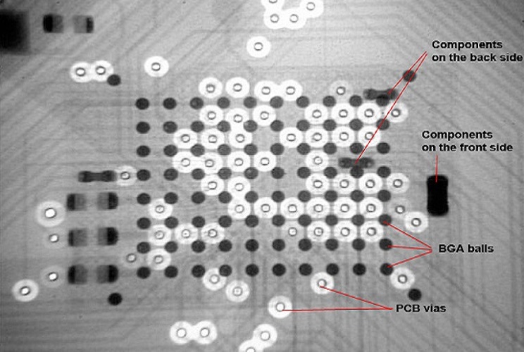
BGA Assembly X-Ray Inspection
We use an X-Ray machine to detect various defects which might occur during BGA assembly. Through X-ray inspection, we can eliminate soldering problems on the board, such as Solder Balls and Paste Bridging. Also, our X-Ray support software can calculate the gap size in the ball to make sure it follows IPC Class II or Class III standards, as per your requirements. Our experienced technicians can also use 2D X-rays to render 3D images in order to check such problems as broken PCB vias, including Via in Pad BGA Designs and Blind / Buried Vias for inner layers, as well as cold solder joints in BGA balls.
Whether your requirement is BGA PCB design, BGA PCB, BGA PCB layout, BGA Assembly or BGA rework, you can rest assured that you will get superior quality and performance, that will in turn, positively impact the performance of your final product.
Thru-Hole Assembly
Through-hole assembly is the process of mounting leaded components to a PCB that involves drilled through holes. Later, the components are soldered to the pads on the opposite side of the board either by manual soldering or automated soldering machine. The solder flux ratio is established carefully as it is essential to maintain the quality of the solder joint between the pad and the component lead. During the THA process, the component leads are inserted from the top of the board to the bottom through drilled holes, followed by soldering. These drilled holes could be plated through holes (PTH) or non-plated (NPTH). PCB manufacturers and designers should stick to IPC 610 A and J-STD-001 for through-hole assembly
Automated Through-Hole PCB Assembly
Why assemble your PCBs using manual through-hole technology when you can have a through-hole PCB assembly company automate and streamline the process? More and more industries use automated technology in manufacturing industries today than ever before. Automated through-hole PCB assembly allows machines to place and solder PCB components faster than employees could do the job manually, which is why the practice of combining manual and machine assembly has become so widespread.
We have a variety of machines that make assembly faster and more efficient. We automate processes using equipment such as the Universal 6287A axial insertion machine, the Hollis Future I SMT and the Ace KISS-103. We are constantly working to integrate new ways to maximize safety, productivity and effectiveness at our company so that we can deliver you high-grade equipment components.
In addition to our machines, we have over 50 individual workstations with ESD protection to maximize safety. We use both technology and human hands to help ensure that the soldering process runs smoothly and that the PCBs we develop and their components will create a strong, durable bond.
Partially automated through-hole assembly saves time and finances while lowering the risk of errors in production. This leads to the use of more reliable equipment and machinery in industries on a global level, which has a positive impact on security and efficiency. As a result, automation has fundamentally changed PCB manufacturing and will continue to influence it for years to come.
Testing Through-Hole PCBs
A large part of manufacturing and assembling PCBs involves the process of testing the products once they have been completed. Living up to quality expectations is important to our company, which is why we have implemented a thorough, accurate testing and inspection method into our business operations.
Assembling electrical components and delivering them to customers without first running them through careful inspection leaves room for error and increases the risk of equipment malfunctions, which slows down operations for businesses. Our automated testing and inspection system catches defects before PCBs go out the door and prevents these types of issues.
At Hemeixin, we use a 2 Mirtec MV-3L optical inspection system that searches for mechanical and manufacturing issues in new PCBs.
Using all these tools, we can accurately detect many types of defects in the design and construction of the PCB through-hole assembly board, such as damage or cracks, inaccurate component placement, incorrect polarity and other potential issues. We only allow our customers to purchase our through-hole assembled PCB services after we have completed the inspection process.
With Hemeixin’s PCB thru-hole assembly services, you can focus on other elements of your industry or company by trusting us to build and test critical electrical components for your equipment. Our thorough testing process protects your investments and helps ensure that the PCBs we offer will act as long-term solutions for your industry.
Mixed Technology PCB Assembly
The mixed technology PCB assembly has the properties of both surface mount technology (SMT), and through-hole technology, hence the name. Thus, these assemblies are most commonly used in the applications, which require the combination of both through-hole and SMT assemblies. This type of PCB assembly does not use any solder paste. Hemeixin is one of the most experienced and reliable manufacturers of these assemblies in the China. We have the capability to manufacture circuit boards with single sided, double sided, as well as multilayer mixed technology.
Mixed Technology PCB Assembly Capabilities
We employ independent automated mixed technology assembly lines for PCBs. This allows us to provide complete PCB assemblies, and prototypes at short turnaround times. Our customers can benefit from our following capabilities:
- State-of-the-art Automated Assembly Equipment
- Automated Laser Sighting and Flux Dispensing
- Fast Production of Densely Populated Mixed Technology Assemblies
- Fast Placement Machines for Ultra-Small and Ultra-Thin Chip Components
- Automated Aqueous Cleaning at Multiple Stages of Production
- Wave and Soldering Machines
- Chassis Wiring and Assembly
Mixed Technology PCB Assembly Testing and Inspection
We follow rigorous testing and inspection procedures, which allow us to ensure high accuracy of circuit boards:
-
Automated Optical Inspection:
Our AOI equipment provides comprehensive fault coverage. It helps us to inspect components thoroughly for their optical placement, orientation, value, color differences, short circuits, dry joints, etc. This is the most effective way of inspecting all mixed technology PCBs, as well as SMT, Through-Hole, and BGA assemblies.
-
X-Ray Testing:
We employ a state-of-the art automated X-ray system to ensure highest quality inspection of PCBs. This type of testing helps us to inspect the quality of PCB components and any hidden faults that are otherwise invisible during visual inspection. This type of testing helps us remove any manufacturing defects in the preliminary stages, and avoid various expensive performance problems in the long run.
-
Functional Testing:
This is performed to ensure the proper functioning of the PCB assembly. Mixed technology PCB Assembly works best for applications that demand surface mount and through-hole components. At Hemeixin, we offer a full range of process and assembly options including assembly on circuit boards with single sided, double sided, flex, and rigid flex, as well as multi-layer mixed technology.
Lead-Free Assembly
The demand for lead-free PCBs is on the rise for varied applications across industries. There are several reasons for the immense popularity of this PCBs, including zero emissions of lead to the environment along with decreased Toxic Release Inventory (TRI). Considering the benefits these PCBs bring, we at Hemeixin produce lead-free PCBs using specific toxic-free components and board finishes. Thus, complying with the RoHS directives, we are also contributing towards reducing e-waste and working towards environmental sustainability. Our lead-free PCB assembly services are offered to those customers who are concerned about the environment and its protection.
Our Lead-Free Assembly services include:
- Lead-Free Materials Analysis
- SMT and PTH Lead Free Board Assembly
- Lead-Free Rigid or Flexible Circuits
- Lead Free Selective Soldering
- Lead Free Wave Soldering
- Lead Free Circuit Board Rework
- Lead Free Encapsulation and Conformal Coating
- Wave Solder Flux Evaluation and Component Evaluation
The lead free SMT Assembly Process
The RoHS PCB assembly process requires that none of the hazardous materials listed in the RoHS Directive are used in the boards, components or solders. Bare printed circuit boards used in the typical "leaded process" are often coated with a lead-tin finish, so the finish on the board must be modified significantly to be compliant with lead-free and RoHS standards.
The lead-free prototype process also requires that boards to be assembled at higher temperatures usually 30-50 degrees or higher. The higher temperature may require the substrate of the circuit board itself and various components to be modified to withstand the higher temperatures in the oven. In addition, the IC moisture sensitivity level that indicates how long the board can be exposed to the air is approximately 2 classes higher for lead-free boards. The shelf life of the materials used in lead-free boards may also be shorter.
Profiling
To ensure proper oven reflow temperature profiling, we ask for one additional lead free PCB along with an extra set of any temperature critical parts; i.e. BGAs, heat slug parts, etc. These can be actual parts, non-functional actual parts or thermally equivalent dummy parts. Most manufacturers of large and expensive components can supply non-functioning "Mechanical Samples" specifically for this purpose. Additionally, suppliers, such as Practical Components provide thermally equivalent parts specifically for this purpose.
Inspection
Due to the metallic composition of lead-free solder, the visual appearance may differ significantly from that of a standard leaded solder joint. Frequently, a first look will give the impression of a cold solder joint. Our inspection staffs are trained to IPC-610D standards to ensure that the solder joints are solid and of high quality.
Starting from temperature profiling, board finish selection and components analysis, board stencil and solder paste application, to component placement, testing, and packaging, we assure compliance with lead-free and RoHS PCB assembly standards. This stringent quality assurance has made us gain comprehensive competitive advantage and huge customer base from industries such as defense, military, marine, electronics, among several others.
On time delivery of quality products has been our motto since our inception. The same is applicable to our lead-free PCB assembly services as well. We own the technique, manufacturing excellence, and the right people, to produce standard as well as customized Lead free PCB assembly beyond customer expectations. Be it a prototype, small or large scale production, we at Hemeixin is equipped to meet the challenges. Additionally, with a highly skilled team of personnel, we ensure meeting the technical specifications given by the customers as it is in the final assembly.
Low Volume PCB Assembly
Low volume, as the term implies, is a batch with limited number of assembly batches. While some OEMs manufacturing electromechanical products require PCBAs in bulk, a low volume PCB assembly may be required for a limited edition product or one with very specific requirements. In such a scenario, it is crucial to first make a low volume prototype PCB assembly as that would give an idea about the final product and if it requires any changes. Hemeixin is an experienced full service electronics contract manufacturer; however, volume has never been an issue for us. We offer PCB assembly services including prototyping even for low volume orders and regardless of the complexity of the requirement.
Low Volume PCB Assembly Capabilities
- Our state-of-the-art facility with advanced tools and machines, experienced teams, and the budget which can cater to low volume prototypes assemblies enable us to achieve low volume PCBs to required specifications. By budgets we mean, we may require tooling for only a small quantity of boards or merely a prototype; however, that is worth the cost and effort as it serves as a future reference for PCB assemblies for many OEMs.
- We have strict testing and inspection procedures in place. The testing techniques include automated optical inspection (AOI), microscopic inspection, x-ray inspection, flying probe test (FPT), and visual inspection.
- We offer single and double sided boards which are mostly flexible or rigid-flex for our low volume PCB assemblies which may comprise barely 200-250 boards or lesser than that.
- For our low volume prototype and PCB assembly, we use different component mounting techniques such as surface mount technology (SMT) and plated through hole (PTH) technology. Additionally, we provide ball grid array (BGA), uBGA/Micro BGA, chip-scale packaging (CSP), and so on.
- We use leaded as well as RoHS-compliant solder types and advanced soldering techniques such as selective wave soldering, pb88 soldering, high melting point (hmp) soldering, and au80 soldering.
- We accept PCB designs in Gerber RS-274X, 274D, Eagle and AutoCAD’s DXF, and DWG file formats. You can share this along with your Bill of Materials (BoM).
At Hemeixin, we understand these difficulties and have made it our goal to raise the bar on our low-volume PCB assembly services to set it apart from our competition. We are pleased to provide the highest levels of quality you would expect from a premier circuit board assembly facility while retaining the flexibility of a low-volume manufacturer.
Kitted PCB Assembly Services
Kitting is the process of putting together a set of components as a kit required to assemble circuit boards. Here the customer provides all the components that go on the board. Kitting brings all the materials/parts into one single package. It is extremely beneficial for the commencement of assembly since all the required components are available, verified, and placed in appropriate packaging.
Every board design and quantity requirements vary according to the customer. Hence, the kit criteria for each assembly project are different. In spite of these, there are particular rules to consider and standards to follow. The analogy could be that of cooking a recipe when all the ingredients are collected either from the market or from the kitchen and pantry. All these ingredients are brought together on the kitchen table and then cooked.
In this type of assembly, a customer provides all components to the manufacturer for assembling. The components to be provided include bare printed circuit boards, electronic components, and all requisite PCB design files, and the manufacturer will assemble the components using automated equipment. This type of PCB assembly is also referred to as consigned PCB assembly. There has been an increasing demand for kitted PCB assembly services, owing to the following reasons:
- This is one of the most economical ways of PCB manufacturing.
- A customer can be assured that components and PCB boards supplied by them are used and no inferior parts are used in the process.
- A customer has better control over the cost of production.
In short, kitted assembly helps OEMs to avoid quality-related issues, and improve their time-to-market capabilities.
Highlights of Hemeixin’s Kitted PCB Assembly Services
At Hemeixin, we offer assistance on the Bill of Material if needed, else we simply accept your list. The Bill of Materials (BoM) is an extremely important aspect of a kitted PCB assembly since it has the list of materials, quantities, minimum order quantity, prices, part numbers, estimated completion time, and so much more. After you provide us with the details, we analyze the details such as feasibility, compatibility with your application requirements, component quality, and so on. We can easily offer you a quote based on your kitted PCB assembly requirements. We off er the following features as part of our kitted PCB assembly services
PCB Assembly Types: We offer the following kitted PCB assembly types.
- Surface Mount (SMT)
- Thru-hole
- Mixed Technology (SMT/Thru-hole)
- Single and double sided SMT/PTH
- Large parts on both sides
- BGA on both sides
- We also support new product introduction (NPI) projects.
PCBA Testing: We carry out in-house testing using manual as well as automated methods at every stage of PCB assembling. This includes functional testing as well as component mounting, the physical design, and so on. Our facility in China is equipped to handle this.
Conformal Coating for PCB Assembly
A conformal coating is a protective film applied to a circuit board that creates a barrier between the contaminants and the board.It acts as an insulation layer and protects the PCB surface at the same time.
Some coatings have a hard texture, while others have a rubbery texture. The conformal coatings are in a liquid state, before the application. These coatings consist of different materials such as acrylics, polyurethanes, silicons, epoxy, or combinations of resins.
Conformal coatings are applied to printed circuit boards (PCBs) to protect them from environmental stress such as salt, corrosion, humidity, and moisture, mitigate tin whiskers, and provide a barrier to electrically insulate components. They enable design of smaller electrical assemblies, while increasing mechanical support for components, and improving the fatigue life of solder joints.
Historically, the only circuit boards going through a conformal coating process were those intended for use in mission-critical applications, like aerospace. Increased popularity surrounding electronic miniaturization and wearable electronics has led to a higher demand for the protection and reliability offered by conformal coating (PCB + electricity + sweat = problems).
Conformal coating is a specially engineered polymeric film-forming product that protects circuit boards, components, and other electronic devices from harmful environmental conditions like moisture, thermal shock, static, vibration, and contamination. These coatings ‘conform’ to the irregular landscape of the PCB providing increased dielectric resistance, operational integrity, and reliability.
If you are an OEM of electrical, electronic or electromechanical devices, and need assistance with regards to kitted PCB assembly, you can totally rely on us. We have an expertise inoffering kitted PCB assembly services.