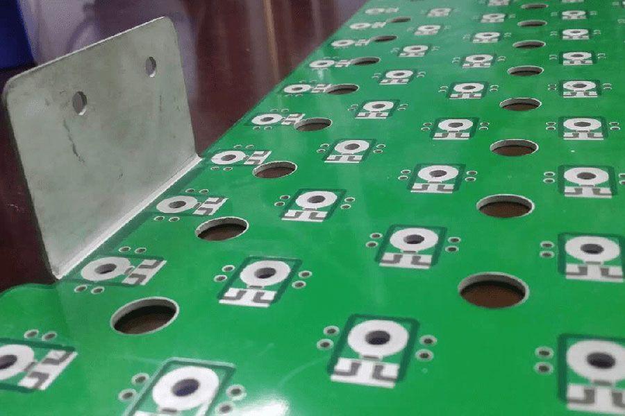
Heavy copper circuit board
The standard high power or high current PCB uses heavy copper. The copper thickness can be very thick like 10 oz. This kind of heavy copper PCB has some limitations like.
-
Difficult in etching process caused low throughput and high cost.
-
Need to use high resin content prepreg during lamination process to fill in spaces between heavy copper pattern.
-
If heavy copper is designed in outer layers, it’s difficult to print solder mask and legend due to uneven surface.
-
Difficult to make finer lines for digital control purpose
-
Uses lots of copper which need to be removed during etching process. The PCB weight is also heavy.
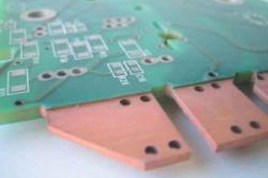
We developed some process for high power automatic application and some 10 oz board and 10+2 oz board in production now. The later one has different copper thickness on the same layer. However, this process is complicate and cost is high. Recently, follow our automotive customer’s requirement, we start to develop the “bus bar” PCB. This technology embeding thick copper bar into PCB for carrying large current. The process is not special to us for we already have lots of experience in coin embedding PCB (please see my other articles). Since many of the high power circuits do not need to use thick copper everywhere. This design can save material cost and PCB weight. Different copper thickness foil can be put into same layer. The resin flows into the thick copper pattern space is also easy. Besides, the bus bar play a roll of heat sink. The high power component can sit on the coin surface for heat transfer.
Since our capability to build coin boards can down to 10 mil thick, similar technology can make bus bar equal or thinner than 10 oz. It can also be designed into mutiple layers. It’s ideally used for design with only less than 10 high current circuits.


