
Heavy copper PCB design guidelines
Hemeixinpcb will check with customers and find out what it requirements are, and match the heavy copper PCB fabrication process to specific needs. It will be important to know for example, the component type, layer count, and material requirements. The Hemeixinpcb can quote the customer and present the pros and cons of using heavy copper. Hemeixinpcb in technology have created a process that utilizes both plating and edging.
Industries that benefit from heavy copper printed circuit boards are military/defense, automotive, solar panel and welding equipment manufacturers, and other sectors that require boards that can handle the heat generated by today’s complex electronics. Another prime industry where heavy copper makes sense is in industrial controls. Heavy copper plated vias are best at transferring heat to an external heat sink. Efficient power distribution is important to ensure high reliability of the PCB and heavy copper allows this to occur.
An increasing number of power electronics products are taking advantage of a growing trend in the printed circuit board industry: Heavy Copper and EXTREME Copper Printed Circuit Boards.
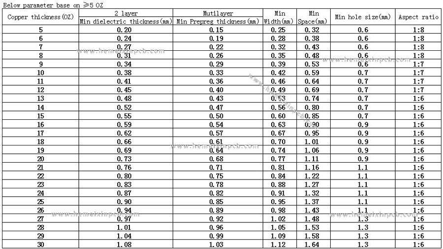
Most commercially available PCBs are manufactured for low-voltage/low power applications, with copper traces/planes made up of copper weights ranging from 1/2 oz/ft2 to 3 oz/ft2. A heavy copper circuit is manufactured with copper weights anywhere between 4 oz/ft2 to 20 oz/ft2. Copper weights above 20 oz/ft2 and up to 200 oz/ft2 are also possible and are referred to as EXTREME Copper. Our discussion will focus primarily on Heavy Copper.
Hemeixinpcb offers heavy copper pcb capabilities, all the way up to what is sometimes defined as Extreme Copper (up to 30 oz.). Discover more about our advanced manufacturing capabilities to meet your unique product demands and design criteria.
Reliable Technology with embedded heavy copper pcb
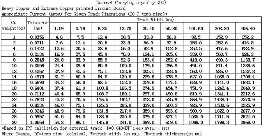
Current Carrying Capacity(DC)
Notes:
The trace width is calculated as follows:
First, the Area is calculated:
Area[mils^2] = (Current[Amps]/(k*(Temp_Rise[deg. C])^b))^(1/c)
Then, the Width is calculated:
Width[mils] = Area[mils^2]/(Thickness[oz]*1.378[mils/oz])
For IPC-2221 internal layers: k = 0.024, b = 0.44, c = 0.725
For IPC-2221 external layers: k = 0.048, b = 0.44, c = 0.725
where k, b, and c are constants resulting from curve fitting to the IPC-2221 curves
Concept to finish or problem specific, design engineers are available to assist our customers. Contact Hemeixinpcb to begin working with the design engineer most able to help you with your heavy copper PCB specific design needs. Please send your email to This email address is being protected from spambots. You need JavaScript enabled to view it. if you want to get some help.


