- Home
- PCB Prototype
- Assembly
- PCB
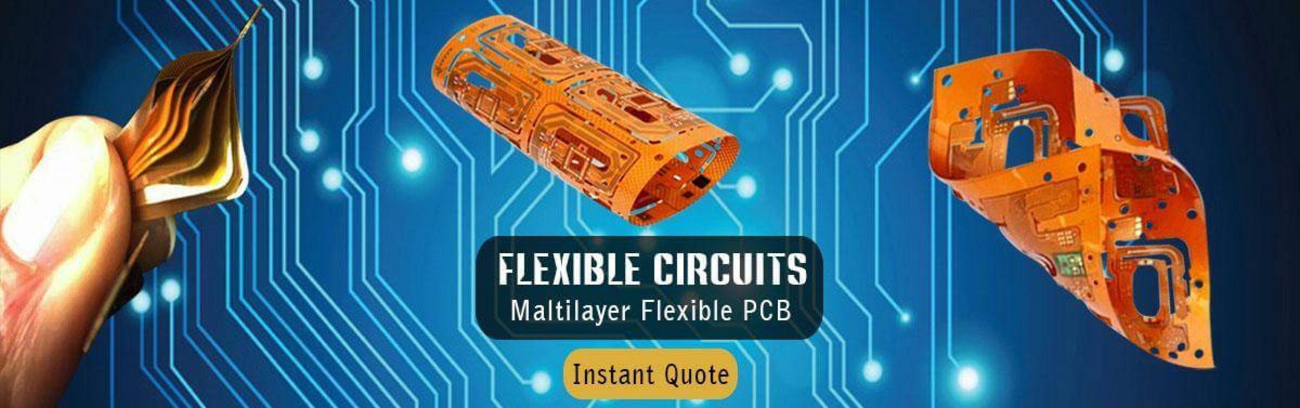
- Rigid-Flex PCB
- Technology
- PCB Material
- Epoxy Filled Vias
- Heavy copper circuit board
- HDI Micro vias PCB
- Controlled Impedance
- RF & Microwave PCB
- Rigid-Flex Circuit
- Bending And Folding
- Thermally Conductive PCB
- Flex PCB Design Guidelines
- Rigid-flex PCB design guidelines
- HDI PCB design guidelines
- Heavy copper PCB design guidelines
- Flexible PCB design issues
- Flex-Rigid PCB design issues
- Turn-key PCB Assembly design issues
- PCB Trace Width Calculator
- Company
- Quote
-
Turn-key PCB Assembly design issues
Turn key PCB Assembly design issues
A CAM hold is a delay in engineering caused by issues in the PCB files submitted for the job. The most common reason for CAM hold is DRC errors in the PCB file. DRC stands for Design Rule Check. A PCB must pass a set of rules in order for it to be manufacturable, such as copper-to-copper spacing, and minimum via hole diameter. The manufacturer provides these design rules to the designer, and the designer uses his/her PCB software to run a DRC on the PCB layout. Any violation of the design rules constitutes a DRC error.
You can help to ensure that your PCBs gets manufactured without being put on hold. Please review these common reason for on-holds.
1. PCB Board basic specification.
- A part number (including revision number) for your design to ease tracking
- Board thickness (.062 inches, .032 inches, .093 inches). .062 inches is standard
- Type of board material (FR4, high-temp FR4, Rogers, Teflon, etc). FR4 is standard
- Number of layers
- Surface finish (SMOBC, HAL, immersion gold, etc). SMOBC and HAL are standard
- The color for solder mask and component overlay. Green is standard
- Copper weight on outer layer (1 oz., 2 oz., etc). 1 oz. is standard
- Copper weight on inner layers (.5 oz., 1 oz.). Either is standard
- The minimum trace and space widths in your design
- Indicate your board dimensions on a mechanical layer
- Do you want your boards to remain panelized, or supplied individually cut?
- Gerber files, drill files, IPC-356A (optional) , X-Y data, Bill of Materials (BOM) in Excel format (for both consigned and turnkey orders)
2. No hole attribute
3. No drill-chart detail
4. NPTH with copper pad
5. PTH without copper
6. Without tooling holes
This board hasn’t bigger non-plated holes. So it can’t support the board during Fabrication and Test processes at Hemeixinpcb PCB Production.
7. Slot size of length<2x width
8. Backdrill hole too small
9. Board thickness mismatch
The specified stackup total thickness does not match finished pcb board thickness.
10. Missing impedance traces
11. Copper extends or pads to the rout profile
12. V-cut to Copper
13. Pad to pad distance <7 mils
Pad to pad distance of less than 7 mils is not enough to build solder mask dams in between pads and at the same time ensure there will be no solder mask on pads.
14. Rogers materials’ solder mask opening.
Due to the ceramic nature type of Rogers material’s, Hemeixinpcb can not run solder mask up to the edges of any routed or scored edge’s with-out chipping the mask during it’s fabrication process. Relieve solder mask 8 mils away from routed or scored edge’s to prevent solder mask chipping.
15. Mirrored texts
16. Silkscreen outside the board
17. Hard gold fingers’ gold thickness
No specified plating gold thickness for hard gold contacts.
18. Netlist mismatch
19. Package mismatch
Provided components of Part number does not match your description.
20. Resistor or Capacitors value mismatch
21. Component is not widely available
Component of xxx is not widely available,It is difficult to purchase. Please provide your alternative part number of components or provide these component from your side.
22. PCB Assembly drawing does not mark polarity information on all polarized parts (cathode, anode, pin number and what the dot or plus sign indicate)
The pcb Assembly Drawing does not specify the Reference Designator Polarity (cathode, anode, pin number and what the dot or plus sign indicate) of XXX.
- Home
- Technology
- Turn-key PCB Assembly design issues


- PCB Technology
- PCB Material
- Epoxy Filled Vias
- Heavy copper circuit board
- HDI Micro vias PCB
- Controlled Impedance
- RF & Microwave PCB
- Rigid-Flex Circuit
- Bending And Folding
- Thermally Conductive PCB
- Flex PCB design guidelines
- Rigid flex PCB design guidelines
- HDI PCB design guidelines
- Heavy copper PCB design guidelines
- Flexible PCB design issues
- Flex-Rigid PCB design issues
- Turn-key PCB Assembly design issues
- PCB Trace Width Calculator

-
Phone:
-
Email:This email address is being protected from spambots. You need JavaScript enabled to view it.