What is Cavity PCB in PCB Design and Manufacturing
What is Cavity PCB?
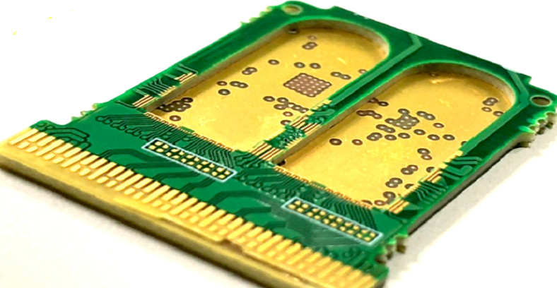
Defined as a hole (Cutouts ) in the PCB going from the outer copper layer to an inner copper layer, but not completely through the PCB.
The use of cavities in a PCB as a method to reduce the component height or to increase component clearances is a viable technology. SMT testing of the cavity boards assembled with the 0.4mm pitch BGA packages at multiple cavity depths has demonstrated that PCBs can be successfully paste printed, assembled, and re-flowed in the same multi-level processes with the existing equipment capability.
Cavity PCB Technology
A Cavity is a cutout in the PCB going from the outer copper layer to an inner copper layer, but not totally through the PCB. The use of cavities in a PCB is a method to reduce the component height or to increase component clearances. It also can be used for real estate constraints and heat requirements, to name a few.
Besides keeping mechanical design in a low-profile format, cavity down can be used to reduce total thickness when inserted components or design for wave guide to reduce signal loss and raise speed of transmission for high-frequency signals, then limiting signal transmission in the slot at the same time.
Cavity PCB Technology Application
Cavities and Coin technologies are used for the boards used in following industries and applications.
- Automotive
- High Current Circuits
- Power Amplifiers
- DC Power Supplies
- Central Electric Hybrid Cars
- Motor Control Modules
- Power-train in EV
- High Speed Computing
- RF & MW Applications
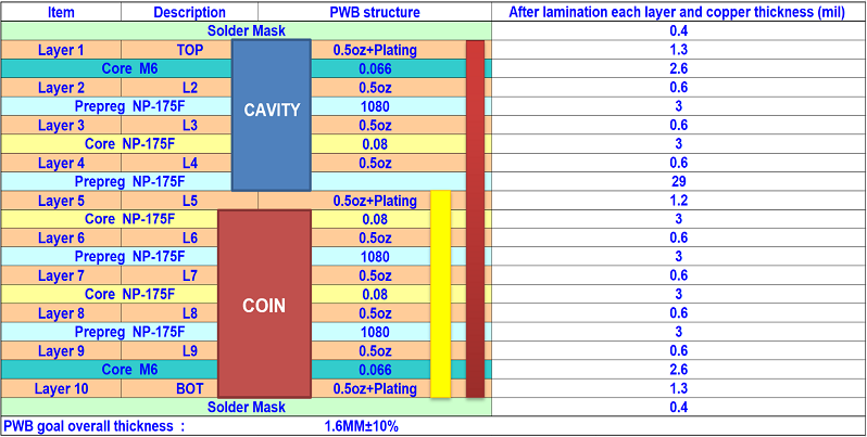
Cavity Process: Lamination (nonflow Prepreg or Adhesive Low Dk Low Df)+depth control milling、Laser depth control mill down
Plated Cavity PCB
A cavity is a recessed opening which allows a component to be placed on a layer other than the top or bottom – essentially a cutout which does not pass all the way through the board. Although cavities can be used for sophisticated RF purposes, and as aids in thermal management, they are most commonly used to save physical space. Components mounted inside of recessed cavities effectively reduce the height of the PCBA. The advantage is that the assembled board will now fit within a slimmer enclosure.
Other more advanced cavities allow for components to be completely embedded. After the component is installed into the cavity, additional materials are laminated over its top, sealing it within the multilayer structure. Placement of the component inside the board frees up space on an external layer, allowing for placement of additional components or circuitry, or for making the board footprint smaller.
Cavity formation requires experience with lamination processes and materials selection. The more consistent the layer thicknesses are, the easier it will be to control the depth of the cut. Accurate machining of the cavity is also critical. Given inevitable variations in material thickness and CNC machine setup, plus the roughness of the copper surface after mechanical milling, it is often necessary to replace mechanical milling with a more controllable laser ablation step.
Laser ablation removes the dielectric material completely, and without chatter marks, leaving the internal layer’s copper surface clean and smooth enough for reliable component mounting. If the layer to be exposed is deep within the PCB structure, then an initial CNC milling step may still be useful. The CNC pass reduces the thickness of the dielectric material in order to shorten the laser cycle time. Then the laser removes the remaining dielectric material for a clean surface. At each step, a good result depends upon the board manufacturer’s equipment, skill, and experience.
Cavity PCB Construction
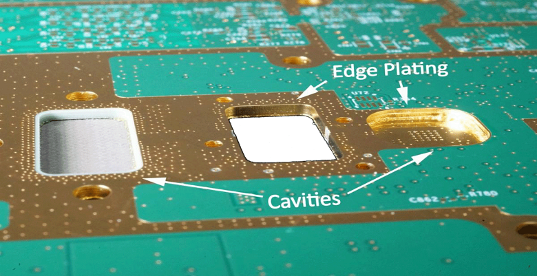
Cavity PCBs have structural recesses to enable additional functionality compared to a standard Printed Circuit Board. This type of feature allows the insertion of heatsinks, often referred to as “coins”, or used to position electronic components below the surface, thereby giving the assembled PCB a thinner overall profile. The inner cavity surfaces can also be used for electrical contact, normally a ground connection. While there are many ways to create a cavity in a PCB, the most common method is by mechanically removing material from a PCB structure to create a “window-type” cavity in a multilayer PCB. As the laminate and prepreg layers are assembled, the layers forming the windows will create the walls of the soon-to-be cavity. If the cavity is functioning as a RF/microwave resonant cavity, the frequency is determined by the size of the cavity and the PCB manufacturer must tightly control the X, Y & Z dimensions of the cavity. Cavity designs can be applied in multiple locations and different depths on a single printed circuit board and can also be edge plated.
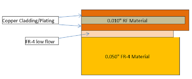
Prepreg Materials
Prepreg is a shorthand expression for "PRE-imPREGnated"; a fiberglass or other fabric reinforcement which has been saturated with a partially cured resin system at the laminate manufacturer. Prepreg is also called B-Stage or Bonding Sheet. When the prepreg is laminated (bonded) in the multilayer package at the PCB manufacturer, the prepreg “flows” under heat and pressure. In a standard multilayer construction, prepregs with “high-flow” characteristics are desired to ensure encapsulation of circuits, filling of holes and elimination of voids. But when bonding cavity PCBs, a “no/low-flow” prepreg is preferred. It is important for designers to understand that even no/low-flow prepregs flow, but the flow can be more controllable and predictable. That being said, it is also important to recognize that the flow characteristics are impacted by the underlying PCB circuit/plane pattern and the configuration of the bonded heat sink.
To compensate for the flow, the PCB manufacturer will engineer the prepreg route program to recess all the edges, so that after lamination the prepreg flows back to the desired position.
Low Flow Prepreg Cutback.
Each no/low-flow prepreg has a unique resin flow percent tolerance which needs to factor into this adjustment. However, even with the best flow characteristic modeling, some trial-and-error lamination cycles may need to be run before the bonding profile can be finalized. Another critical consideration is that some flow bleed into the cavity is desired to assure complete bonding. By collaborating with the PCB manufacturer, RF pcb designers can avoid selecting bonding materials that lack good flow control and might flow into the resonant window or cavity area. In a resonant cavity design, changing the dimensions of the resonant cavity will change its operating frequency.
Cavity PCB Design Considerations
- Cavity designs should utilize no/low-flow prepreg
- Acceptable bleed into cavity needs to be defined; IPC 6018 allows .029”
- Critical Registration: special tooling, fixturing and bonding profiles are required
Cavity PCB creation
At the cutting edge of tomorrow's technology
End devices are becoming smaller and smaller, and the space on the printed circuit boards is becoming more and more precious. For a long time now, it has no longer been sufficient to assemble the outer layers conventionally, and the inner layers (multi layers) are also being used.
Cavities make it possible to accommodate components in the inner layers and thus to fit increasingly complex assemblies in a smaller space.
By utilizing several layers, the space on the same area can be utilized to the maximum.
In order to place micro chips, heat sinks or resistors on the circuit boards, recesses, so-called cavities, are made in the circuit board by means of a laser in order to remove the desired material.
The laser first opens the copper surface and then removes the dielectric. Another laser pass cleans the exposed inner copper surface from resin residues.
We provide various package printed circuit boards and module PCBs with cavity structure exposing selected inner layer patterns (bonding pads, ground layers, etc.) on multi-layer PCB and build-up PCB.


