ATE PCB boards and Probe card PCB
We have over 10 years of experience producing automated test equipment (ATE) boards for leading companies.
Automated Test Equipment (ATE) boards are used in the semiconductor chip testing process. ATE boards are increasing in complexity with greater numbers of layers – upwards of 40 to 60. These designs focus on high complexity, high performance, and high layer count.
ATE PCB (Automated Testing Equipment Printed Circuit Board) can be your answer to testing highly complex devices! With advancing technology, the one thing that becomes imperative is to test highly complex devices in order to ensure reliability. An effective way to do it is viding an automatic test equipment printed circuit board or ATE PCB. It acts as an efficient way to test large test systems.
When it comes to ATE PCBs, any small error can lead to not just monetary loss as well as lost time-to-market. It is imperative, therefore that the ATE PCB program managers have specialized skills that go beyond conventional PCBs.
Our worker staff has decades of knowhow and experience to efficiently complete the most complex ATE PCB board manufacturing. At Hemeixin, you’ll get the best and most effective ATE PCB fabrication our industry offers. Contact us for a complimentary consultation.
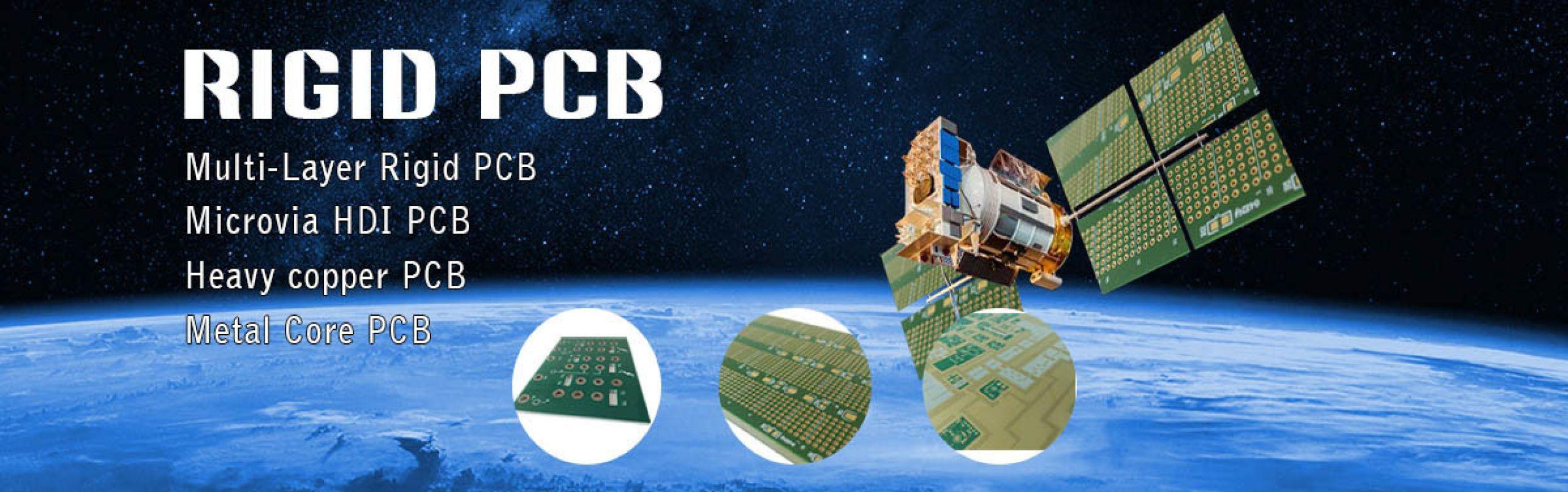
Probe Card PCB
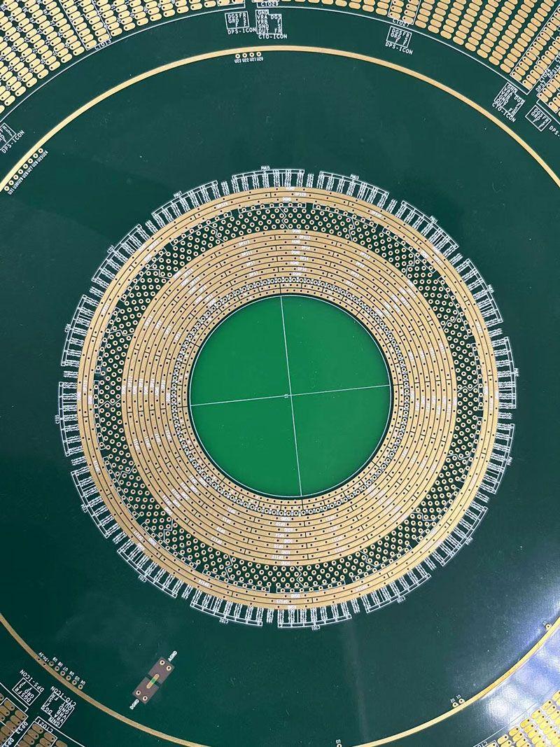
Used to test the un-cut, un-packaged semiconductor, that is performing the electrical test for Die;The PCB BGA pitch is usually ≥0.3mm, when pitch <0.3mm, need to use interposer and MLO adaptor board to connect with probe card; Impedance controlled and highly demanded for surface evenness.
Vertical (advanced) probe card
A probe card is essentially an interface or a board that is used to perform wafer test for a semiconductor wafer. It is used to connect to the integrated circuits located on a wafer to the ATE (Automated Test Equipment) in order to test their electrical parameters and performance before they are manufactured and shipped out.
Vertical probes are probe cards that are used to perform multi die testing of the likes of products associated with general logic and microcomputers. The needles are short and are positioned vertically when compared to the substrate, making it an ideal choice for small pad and high frequency wafers.
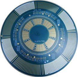
Burn in board
Used for performing aging test for packaged IC under certain working environment and time, to verify the reliability; BGA pitch is usually≥0.4mm, with polyimide material which got ultra-high thermal performance.
Burn in Board is a printed circuit board which functions as a jig in the Burn-in process. The Burn-in Board is used as part of the ASIC reliability testing process during which components are stressed to detect failures. Burn in Boards consist of sockets to accommodate the tested ASICs and are designed to withstand the hot temperatures during tests.
Load board
Through cut, Die attach, wire bonding, plastics package, wafer will be packaged by epoxy resin or other material, becoming IC. And then ATE machine will perform the electrical test to verify the good and bad; BGA pitch is usually≥0.35mm; Impedance controlled.
LoadBoard (LB) is a mandatory, custom made PCB, that acts as a mechanical and electrical interface between the tester (ATE) and the device under test (DUT). LoadBoard has well-defined physical dimensions and it must fit perfectly into the tester. It is one piece of the entire ASIC Test Solution and it should be specified in the ASIC Test Specification Document. The image shows a Loadboard with a Socket and a Stiffener.
Generally speaking, a LB consists of 2 interfaces: One interface is upwards to the tester’s handler unit. The hander is an automatic pick and place unit that takes the DUT from the tray and place it into the socket. The second interface is downwards to the tester’s pogo pins. These are the tester IO ports that electrically connect the tester to the DUT.
ATE LoadBoard (LB) design
Load Board is used for the purpose to interface between Tester and device to evaluate the electrical feature. Main performance is the analyzing the electrical of the board.
Load board design takes into consideration many factors, one of which is power supply routing. It is good practice to assign a separate power plane for every supply voltage needed by the DUT, even if two or more supplies will be tied up to the same nominal voltage. This has two advantages:
- noise immunity between power supplies
- the ability to assign each power supply to a different voltage later on.
Adding sense lines as close as possible to the DUT to each power plane for output monitoring would also be helpful. Put decoupling capacitors between each power supply pland and the ground plane to reduce power supply noise. Note that the values of the capacitors must be chosen based on the operation frequencies of the DUT.
Signal routing is another consideration in the design of a load board. Avoid overlaying power supply planes over signal planes. There are two types of DUT signals, and guidelines for handling them in a load board differ. The first type, the low-speed digital signal, doesn't require much as far as load board design goes. Digital signals can share the same plane, but they should have their own plane. The lengths of their traces should be the same.
The second type of DUT signal is the high-performance signal. This signal type requires high-performance instrumentation for measurement, because the speed and accuracy of these signals could not be handled by the ATE. Keep the length of the cable connecting the DUT to the load board as short as possible. Avoid parallel runs of mixed signals as well, to avoid noise coupling. Needless to say, high-performance signals need a signal plane of their own.
Load boards require connectors for cables that run to the test site. High-speed applications commonly employ SMA and SSMB connectors. Higher bandwidth applications are better off using the SMA connector, since this screw-on/screw-off type of connector is larger and designed for higher bandwidth than the SSMB connector, which is a push/pull type of connector. SMA is also sturdier on the load board and can withstand a greater deal of mechanical stresses.
Decoupling capacitors must be placed as close to the DUT as possible - preferably directly under the socket. AC coupling capacitors and termination resistors must likewise be as close to the DUT as possible. The use of surface-mounted components is also recommended for load boards. Power supplies used for load boards must have enough power to energize all relays on the board.
ATE LoadBoard (LB) Manufacturing and Production
Semiconductor load boards are a crucial part of IC production quality control. Load boards often have complex designs because they provide a range of electrical connections to the ICs to measure several parameters, such as current, voltage, and power. Moreover, load boards often need to support high-speed signaling, which requires careful routing of the traces to minimize signal loss and crosstalk.
Load boards are often customized to a specific device or group of devices. As such, complete, ready-to-use load boards are not normally available off-the-shelf. The usual way to acquire a load board for a new product is to have it designed and fabricated. Thus, most test engineering groups have a certain level of expertise in designing and fabricating a load board.
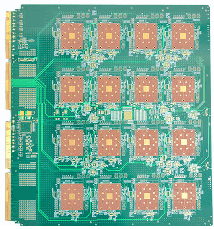
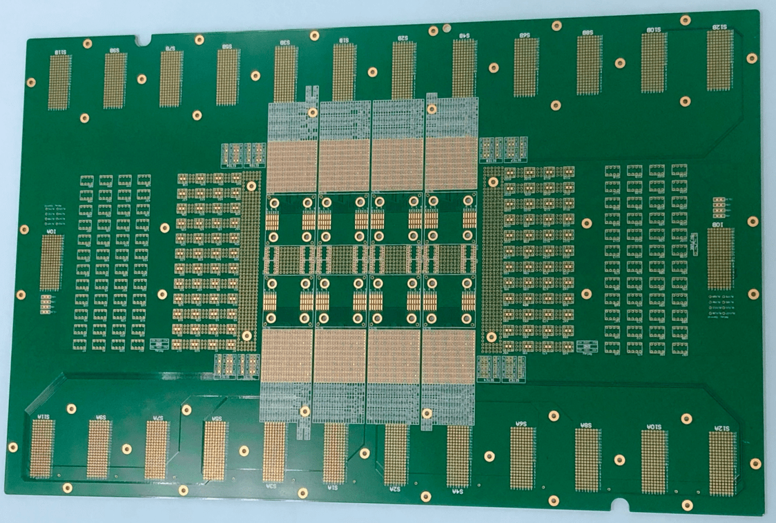
A load board consists of a PCB with a test socket or handler interface as well as a variety of components (IC's, resistors, capacitors, inductors, relays, connectors, etc.) that make up the load board's test circuits. The typical laminate for the load board PCB is the FR4 (Flame Retardant 4 fiber glass). The number of layers of a load board PCB also varies, depending on the complexity of the design. Some load boards for complex devices may even have more than 20 layers.
LoadBoard design consideration are similar to any other PCB. Power supply distribution, clock signals routing , high speed signals routing, signal integrity, wire length all this design rules applies here too. In some cases, it’s sensible to run some electrical simulation, especially to ensure RF signal performance.
The next phase after layout is successively completed is of course manufacturing/fabrication of the board services and assembly of the board with the various passive or active components and socket.
We always recommend building 2 boards instead of just one because we use the 2nd board as a backup in case there is a failure in the 1st board. These type of failures can stop an entire production line, therefore to lower the risk of delays in production and shipping you may want to consider having a backup LoadBoard. LoadBoard fabrication and assembly could take up to 8-10 weeks depending on the design complexity.
Loadboard is an essential part of the ASIC test solution. Make a robust but yet simple design to ensure minimum production problems, keep one board as a backup if you can afford it.
An ideal load board introduces no distortion, noise, delays, nor errors to the testing process of the DUT. This means that an ideal load board is one that doesn't seem to exist at all, i.e., as if the DUT were directly connected to the ATE. To come out with a load board as close as possible to this ideal one is the challenge to every engineer who designs load boards.
ATE PCB and Probe card PCB Capabilities
| Item | Standard Technology | Advance Technology |
|---|---|---|
| PCB Thickness | 250 mils | 280 mils |
| PCB layer count | 60 | 80 |
| Min Impedance Tolerance | ±5% | ±5% |
| Min Finished Thickness Tolerance | ±7 mils | ±7 mils |
| Min Dielectric Space | < 1 mil – 0.5 mil | < 0.5 mil |
| Drill Pitch | 14mils | <14mils |
| Min Drill Hole | 5mils | 4mils |
| Min Aspect Ratio | 42:1 | 46:1 |
| Min Drilled Hole to Copper | 3 mils | 2.5 mils |
| DUT Pin Count | 1500-2000 | >2000 |
| Stub Drill Pitch | 87mils | 87mils |
| Min Internal Line Width | 1.75 mils | <1.75 mils |
| Min Internal Space Cu to Cu | 2 mils | 1.5 mils |
| Min External Line Width | 2.2 mils | <2.2 mils |
| Min Extenral Space Cu to Cu | 2 mils | 1.5 mils |
| Warp&Twist | 0.5% | 0.3% |
| POFV evenness | 15μm | <15μm |
| DUT pads height difference | / | 1.5mils/inch |
| Whole pads height difference | 200μm |
ATE PCB TEST
| Requirements | Description |
|---|---|
| Alignment&High aspect radio | Main trend load board BGA pitch is 0.35~0.5mm; Multiple parallel test channels: 4site 8 site~16site; >30 layers, space between holes and conductors is under 4mil; PCB capability requirements: high layer precise alignment and drilling, plating and VIA IN PAD for high aspect radio. |
| Test Interface | Main trend Probe Card BGA pitch is 85~200um; High-end is 40~55um, which is beyond the PCB processing capability, need to use MLO/MLC space transformer interface, with ICS and wafer backend technology. |
| Surface evenness | Probe Card and high-end ATE board request high surface evenness performance, warp and twist is 0.1%~0.2%, DUT Area pads height differences should be controlled in 2 mils, high-end products request 25-28um |
| Surface Quality | DUT area pads need to connect through probe, thus the pads surface have to be high performance, no cave, no damage, no scratch, and no roughness etc... |
| Signal Integrity | To confirm signal integrity, need to confirm impedance at ±5% tolerance and back drill stub <10 mils; Need high capability of plating and etching uniformity and back drill processing. |
ATE PCB Technical Feature
Hemeixin’s expertise in the manufacture of ATE pcb board hardware runs both broad, and deep. Hemexin has specialized manufacturing teams with knowledge and experience across all the major Technical Features. The manufacturing and test process for ATE boards at Hemeixin is honed to produce the highest in quality and reliability. Hemeixin’s customer base in this business sector includes several of the world’s leading semiconductor companies and serves as testimony to its success and commitment to customer satisfaction in this area.
At Hemeixin, we are equipped with the state-of-the-art equipment as well as an expert team that can handle the most specialized requirements for ATE PCBs. Additionally, when you join hands with us you also get access to a rich body of industry best practices that give you an edge.
We are extremely committed to offering quick turnaround times that help you go-to-market early. The fact that we have an unstinting focus on quality endears us to our clients.
All you need to do is to get in touch with our team and share your bespoke requirements. Our experienced team will share a custom quote that is extremely cost-effective and ensures that your project is extremely competitive!
Hemeixin has specialized ATE pcb manufacturing teams with knowledge and experience across all the major tester platforms. The ATE PCB manufacturing process for ATE boards at Hemeixin is honed to produce the highest in quality and reliability.
Type of ATE PCB:
- Epoxy Probe cards, Blade Probe cards and specialty Probe cards.
- Device Interface Boards
- Handler Interface Boards
- Prober Interface Boards
- Load Boards
- Bench Boards
- Evaluation Boards
- Reference Boards
- Adapter Cards
- Burn in Boards
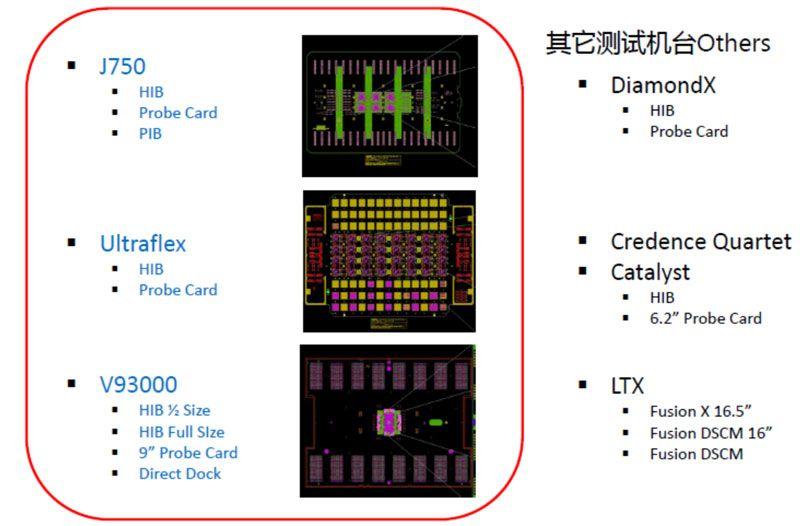
ATE Tester types
Load Boards
|
Advantest Load Board |
Credence Load Board |
Teradyne Load Board |
Verigy Load Board |
|
T6672 |
ASL1000 |
CATALYST |
V93000 |
|
T6372(ND2) |
ASL1000-D10 |
J750 |
V83000 |
|
T2000 |
ASL3000 |
ULTRAFLEX |
|
|
T6673SQ |
ITS9000 |
FLEX |
|
|
T6673ZIF |
PKII |
TIGER |
|
|
QUARTET |
D750EX |
||
|
EXA3000 |
|||
|
FUSION CX |
|||
|
FUSION HF |
|||
|
SC312 |
|||
|
SAPPHIRE |
|||
|
SAPPHIRE-D10POGO |
Advantest Probe Cards
| T2000 |
DUO9 |
CATALYST | TIGER |
|
T5335P |
SC312 |
J750 |
J971 |
|
T5371 |
KALOS2 |
IP750 |
V83000 |
|
T5377 |
ASL3000 |
D750EX |
V93000 |
|
T6371P |
SAPPHIRE |
ULTRAFLEX |
V93K-INT-PC |
|
T6372(ND2) |
SAPPHIRE-D10 |
FLEX |
TS6700 |
|
ST6730 |
Having vast experience in working for all major test board and ATE IC test system Customers. We have long experience in manufacturing PCB boards for ATE under different PCB design requirements and able to provide high yield manufacturing solution.
ATE PCB fabrication process adopted by the experienced professional manufacturer ensures right PCB delivered at first pass on schedule.
Burn-in Boards
Burn-in is a process done to components prior to regular use in which the components are stressed to detect failure and ensure component reliability.
The PCB burn-in process is usually done at 125ºC, with electrical excitation applied to the samples. The process is facilitated by using burn-in boards where the samples are loaded. These boards are then inserted into the burn-in oven which supplies the necessary voltages to the samples while maintaining the oven temperature at 125ºC. The electrical bias applied may either be static or dynamic.
What is Burn-in Testing?
Burn-in testing helps PCB manufacturers analyze how well a new board can handle excessive use and heat and whether these factors will lead to functional errors. Each board works within specific current and internal and external temperature parameters. Burn-in testing pushes these boards to the point where they usually fail to see whether these issues arise.
During burn-in testing, technicians run a current through a prototype board, operating the board’s firmware while it is held in a high-temperature environment. This typically happens for between 48 and 168 hours. The manufacturer then examines the board’s functionality to see what issues arose and whether any components or firmware failed. If defects occur during a device’s earliest days of use, you’ll get ample time to examine and rectify them.
Types of Burn-In Testing
Manufacturers use two main types of burn-in testing: Static and dynamic. They each provide different stressors and are necessary depending on the board’s intended uses.
Static Burn-In Testing
Static burn-in is the cheaper and quicker option that tests the board against a single criterion, typically heat or voltage. Testers run probes across the board from component to component in a temperature-controlled environment. Once the test chamber is up to the required temperature, the probes run a steady current through each component at a chosen voltage.
The point of this test is to examine the results of constant exposure to, or stage within, extreme temperatures. Static testing is ideal for boards stored in warm climates or machinery that runs at a steady high temperature. Each component is tested to determine the effects of this exposure, allowing them to be replaced should an error or defect arise.
Dynamic Burn-In Testing
Like static burn-in testing, dynamic trials involve setting a testing chamber at the desired temperature and running a current through each component. The main difference with dynamic testing is that the components also run input signals into each element. This tests the components against voltage and temperature resistance and allows the tester to see the effects these have on the components’ functionality.
Dynamic testing is best for boards operating in extreme environments or under heavy strain. These trials find malfunctioning components that need to be removed before later testing, cutting down on other errors. They also allow testers to see how much the firmware is affected.
Regardless of the test type, ideally, you want to perform burn-in testing multiple times to ensure reliable results. As these examinations examine the possibilities of errors over time, you’ll get the best results from the most prolonged time frames.
Board Materials
Burn-in boards are made of high-grade materials. To withstand the oven testing reaching 125ºC, a special version of FR4 is used (High Tg FR4). For temperatures reaching up to 250C, a polyimide is used and for higher temperatures of 300C, a higher grade of polyimide is used.
Burn-in Board Design
The burn-in board design is similar to your typical PCB design guidelines, however, there are some additional factors. One of the most important aspects to consider is selecting the highest possible reliability and quality for the burn-in board and test socket. The last thing you need is it failing before the device under a test. All active/passive components and connectors should comply with high-temperature requirements, and all materials and components should meet high-temperature and aging requirements.
LoadBoard Design rules
Load board design takes into consideration many factors, one of which is power supply routing. It is good practice to assign a separate power plane for every supply voltage needed by the DUT, even if two or more supplies will be tied up to the same nominal voltage. This has two advantages: 1) noise immunity between power supplies and 2) the ability to assign each power supply to a different voltage later on. Adding sense lines as close as possible to the DUT to each power plane for output monitoring would also be helpful. Put decoupling capacitors between each power supply pland and the ground plane to reduce power supply noise. Note that the values of the capacitors must be chosen based on the operation frequencies of the DUT.
Signal routing is another consideration in the design of a load board. Avoid overlaying power supply planes over signal planes. There are two types of DUT signals, and guidelines for handling them in a load board differ.
The first type, the low-speed digital signal, doesn't require much as far as load board design goes. Digital signals can share the same plane, but they should have their own plane. The lengths of their traces should be the same.
The second type of DUT signal is the high-performance signal. This signal type requires high-performance instrumentation for measurement, because the speed and accuracy of these signals could not be handled by the ATE. Keep the length of the cable connecting the DUT to the load board as short as possible. Avoid parallel runs of mixed signals as well, to avoid noise coupling. Needless to say, high-performance signals need a signal plane of their own.
Load boards require connectors for cables that run to the test site. High-speed applications commonly employ SMA and SSMB connectors. Higher bandwidth applications are better off using the SMA connector, since this screw-on/screw-off type of connector is larger and designed for higher bandwidth than the SSMB connector, which is a push/pull type of connector. SMA is also sturdier on the load board and can withstand a greater deal of mechanical stresses.
Decoupling capacitors must be placed as close to the DUT as possible - preferably directly under the socket. AC coupling capacitors and termination resistors must likewise be as close to the DUT as possible. The use of surface-mounted components is also recommended for load boards. Power supplies used for load boards must have enough power to energize all relays on the board.
A properly designed LB is electronically “invisible”, and does not introduce any distortion or delay to the DUT signals. The LoadBoard should be able to support all the tests executed on the tester and be flexible enough to support future testing (for example expanding the test solution to support quad parallel testing).
In fact, many test engineers try to avoid having any active components on the LB but rather have only the necessary passive components to support the ASIC functionality. The trend of simplifying the LoadBoard is coming from need to decrease the probability of failure in production phase that can stop production line. The time of fixing a bug increases when the LoadBoard is complex.
Different testers (ATEs) require different LB size. But they all LoadBoards consist of the same elements:
- Socket for the DUT ASIC
- Interface pads for the tester
- Stiffener – adding mechanical strength
- Some components per DUT requirements (R, C, etc)
- Connectors for the debug phase
In some cases, in addition of being an interface board the LB can also contain on board testing capabilities (e.g. such as FPGA). When the tester alone cannot support some specific testing task these could be performed directly on the LB (such as loopbacks).
Almost any layout or PCB engineer can design a LoadBoard, there are no special requirements besides the general understanding of the test and LoadBoard concept. A LB is typically made of RF4 material and normally very thick and consist of 20 layers or more.
LoadBoard design consideration are similar to any other PCB. Power supply distribution, clock signals routing , high speed signals routing, signal integrity, wire length all this design rules applies here too. In some cases, it’s sensible to run some electrical simulation, especially to ensure RF signal performance.
The next phase after layout is successively completed is of course manufacturing/fabrication of the board services and assembly of the board with the various passive or active components and socket.
We always recommend building 2 boards instead of just one because we use the 2nd board as a backup in case there is a failure in the 1st board. These type of failures can stop an entire production line, therefore to lower the risk of delays in production and shipping you may want to consider having a backup LoadBoard. LoadBoard fabrication and assembly could take up to 8-10 weeks depending on the design complexity.
Loadboard is an essential part of the ASIC test solution. Make a robust but yet simple design to ensure minimum production problems, keep one board as a backup if you can afford it.


