
Flex PCB Bending And Folding
Flex circuitry is ideal for many of today’s electronics needs. It is light, compact, and, if properly designed,extremely robust. Because it bends, however, a flex circuit has some very specific requirements that aredifferent from those of traditional rigid circuits. Materials, circuit architecture, placement of features, and thenumber of layers in the circuit must all be considered in the design process. So must the degree to which thecircuit will be bent, how tight the bend will be, how the bend will be formed, and how frequently the circuit will be flexed. By carefully defining the application and design priorities and recognizing the unique demandsmade upon flex circuits, the designer can work within these requirements to realize the technology’s fullpotential.
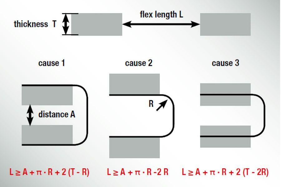
Calculation of flex pcb length
The most frequently asked question we receive regarding flex circuits is “how much can I bend a flex?” The standard IPC answer is 10 times the thickness of the material. There is a section in IPC-2223 that offers reasonable information on bend radius calculations. But there are other factors that need consideration when designing a flex circuit for high reliability.
With Short flexible areas, four bonded flex layers are easier to bend than 2+2 flex layers with airgap.
A variety of factors can impact a circuit’s performance when flexed. These include:
- The closer the neutral bend axis falls to the center of the circuit’s material stack, the more evenly forces will be distributed among the other layers of the circuit when it is flexed
- Bend angle – the less a circuit is flexed, the smaller the risk of damage
- Thickness of the circuit – less thickness reduces the risk of damage when flexed
- Bend radius – a larger radius helps reduce the risk of damage
- Frequency of flexing – construction that might not be acceptable for a dynamic application, one in which the circuit will be flexed regularly, may be acceptable in a circuit designed to bend only once for installation
- Materials – proper selection of materials for their ability to accommodate flex and the way they transmit those forces to other layers in the bend area will improve performance
- Construction – designers should avoid placement in or near the bend area of features that are particularly vulnerable to forces generated in the bend area, or that can weaken surrounding circuit structure when flexed
We performed a manufacturing cost simulation with a real rigid-flex circuit designs and a comparative rigid-cable-rigid equivalent. The component BoMs for comparison differed only in the cable and connectors required for the non-flex version. For our simulation, the traditional design is comprised of four-layer boards that use flexible cable and connectors between them, while the rigid-flex circuit design is a four-layer PCB with two inner flex layers. Manufacturing cost for both designs is based on real PCB fabricator quotes, and includes the cost of assembly.
REDUCE FLEX PCB OVERALL THICKNESS IN THE FLEX AREA
- Reduce the base copper weight (and the corresponding adhesive thicknesses) or reduce the dielectric thickness.
- Use adhesiveless base materials. Adhesiveless materials will usually reduce the starting thickness of each substrate by 12-25um (0.0005”- 0.0010”) when compared to adhesive based substrates.
- Eliminate copper plating on the conductors in the flexing area (dynamic region) by utilizing selective (pads plating/button plating-only) allowing the circuit to have increased flexibility.
Fully Bonded Vs Air Gap Constructions
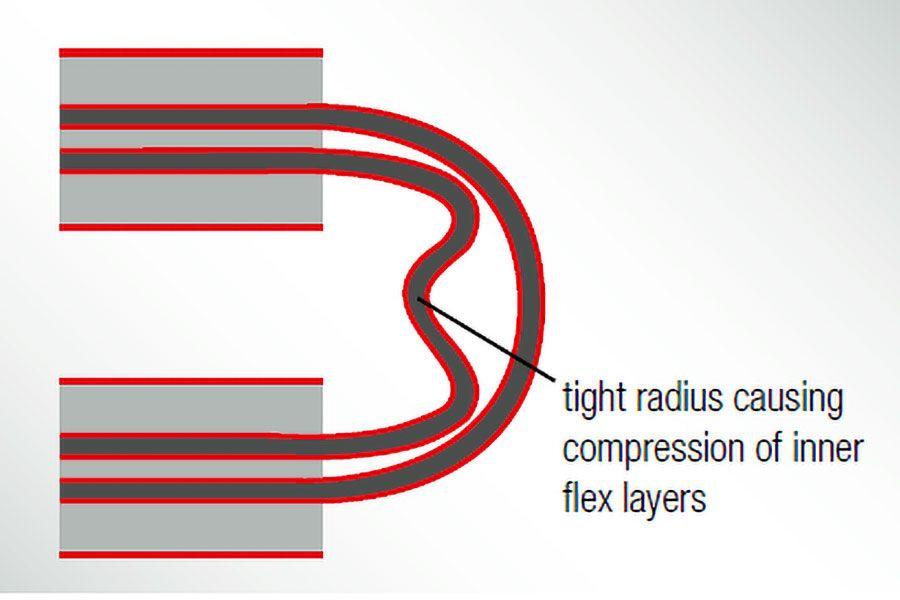
Higher layer count designs may need to utilize an Un-bonded Air Gap construction, a technique which configures layers as separate pairs, as opposed to a single fully bonded unit. The thinner individual pairs provide a higher degree of flexibility.
How air gap construction improves mechanical flexibility and bend capability

An air gap architecture considerably improves the bending capability of flex pcb boards. The following two factors are responsible for these improvements:
1. The flex thickness of each individual flex layer is significantly reduced when compared to a totally laminated construction. This not only improves the flexibility but also reduces the IBeam effect.
2. Each flex layer is permitted to bend independently based on its thickness, with little interference from the other flex layers.
Individual flex layers are allowed to bend to their natural radius. As the air gap space between layers is exhausted, they may get into contact with each other. In an extreme U-shaped bend requirement as shown in the image above, the outer flex layer may confine the inner flex layer till it buckles. Any buckling of a flex layer beyond the material’s capabilities would result in fractured circuits, hence this circumstance must be avoided.
Routing for Rigid-Flex PCB Boards Bending
In regard to your traces and routing, keep your traces as straight, perpendicular lines. If your board bends or folds along a horizontal line, then have your traces run vertically. Traces should ideally go in one direction, but in the case where changing directions is a must, curve the traces as opposed to sharp 45 or 90 degree corners. This will eliminate high-stress areas from your board. Use narrower traces that are evenly spread out across a flexible pcb area to decrease areas of high stress. Adding in dummy traces or even redundant traces can help increase the mechanical sturdiness of the flexible areas and protect traces from breaking the signal path completely. In the case of traces on both the top and bottom of a flexible section, alternate them such that a bottom layer trace has no top-layer traces immediately above it, and a top layer trace has no bottom-layer traces immediately below it.
Cross-hatching: is a form of non-solid ground plane that aids in flexibility of the ground a solid area will not allow the flex to bend.

For your power, signal, and ground planes, if you pour a typical plane with a solid area of copper, you’ll end up putting a significantly large amount of stress on your board and reduce its flexibility. Instead, use a hatched-polygon pattern for the plane. Minimize your trace widths on the fill as well, but be aware that a cross-hatch isn’t great for high-speed signal integrity.
Because the IPC standards are conservatively written to take into account many factors that can affect circuitresilience, it is possible to safely achieve lower-than-standard bend ratios. However, due to the number offactors that can affect performance at smaller-than-recommended bend ratios, it is highly advisable thatdesigners work with an experienced flex circuit manufacturer in developing such designs.


