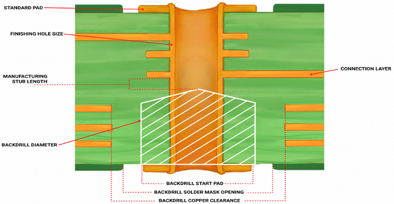
Backdrilling in PCB Manufacturing parameters and design rule
What is backdrilling PCB?
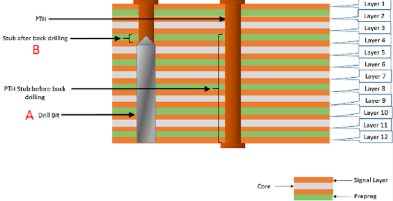
Controlled Depth Drilling (CDD), also known as back drilling, is a technique used to remove the unused portion, or stub, of copper barrel from a thru-hole in a printed circuit board. When a high-speed signal travels between PCB layers through a copper barrel, it can be distorted. If the signal layer usage results in a stub being present, and the stub is long, then that distortion can become significant.
These stubs can be removed by re-drilling those holes after the fabrication is complete, with a slightly larger drill. The holes are back drilled to a controlled depth, close to, but not touching, the last layer used by the via. Allowing for fabrication and material variations, a good fabricator can back drill holes to leave a 7mil stub, ideally the remaining stub will be less than 10mil.
If the functional portion of the PTH is connecting two internal layers, it may be necessary to remove the stub from both the top and bottom of the board.
Backdrilling PCB technology
For high frequency applications we need to prevent signal loss and therefore when one layer is connected to another and the signal travels from one layer to another it must pass through a via hole that connects the layers. If the signal is to pass layer one to layer two in a 20 layer board, for example, then part of the via structure is considered as ‘excess’ and for this application it is best to remove the excess copper from this hole as it acts as an antenna and impacts the signal.
We use back-drilling (controlled depth in z-axis) to drill out the ‘excess’ copper in the hole in order to get better signal stability. Ideally the shorter the stub (‘excess’ copper) then the better the result. Back-drill size should be typically 0.2mm larger than corresponding via.
|
BACK DRILLING (mm) |
Parameters |
|
A: Depth tolerance |
+/-0.10 |
|
B: Min. remain thickness and tolerance |
0.15+/-0.1 |
Backdrilling PCB drill table
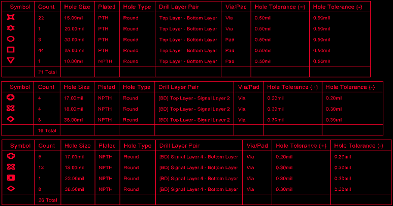
A placed drill table can be configured to show all drill layer pairs, or it can be configured to show a specific layer pair. The image below is from a design with back drilling from both the top and bottom sides of the board, so three tables have been placed. Note the Drill Layer Pair column; it indicates the function of each table.
Backdrilling in PCB Manufacturing
Plated through holes (PTH) are great. They electrically connect two or more layers together, and serve as convenient connecting points for traces and components throughout a multilayer PCB. PTHs are mechanically sound, and can also be used as mounting holes.
But there’s a dark side to PTHs. Often times you don’t need the via to run the entire thickness of a board. The unused portion of the PTH that serves no functional purpose to the circuit is called a stub. And in high signal circuits, it can become significant source of signal distortion.
If your PCB is suffering from deterministic jitter, a high bit error rate (BER), signal attenuation, and other EMI problems, backdrilling may be the solution you’re looking for. In this post, we’re going to cover backdrilling, a handy technique for removing problematic stubs from PTHs.
Backdrilling PCB DFM tip
The back drill diameter needs to be slightly larger than the primary drill diameter. The back drill bit size (diameter) is usually 8 mils over primary drill size, with 10 mils larger preferred. Trace and plane clearances need to be large enough that the back drilling process does not accidentally drill through traces and planes located adjacent to the back drilled hole. Minimum plane and trace clearances (spacings) of 10 mils are preferred.
Backdrilling PCB from a manufacturing perspective
You can note that alternate construction techniques could also be used to minimize stub length. These include laser-drilled vias (microvias), or blind and buried vias, and alternative stack-up arrangements - where traces are moved to layers closer to the end of the via stub. Also, back drilling is not necessary for high frequency PCB (greater than 3GHz) boards since alternative strategies are used to reduce signal reflection.
However, in many high-density PCBs and backplanes/midplanes, these options are not always viable from both manufacturing and cost standpoints. In such a scenario, the only option is to remove the via stub by back drilling. Back drilling is necessary for high frequency (greater than 1GHz within 3GHz) boards when blind vias are not viable.
Advantages of back drilling PCB PTH vias
- Via stubs give rise to a signal distortion issue named deterministic jitter. Jitter with regard to signal transmission in a PCB refers to timing errors caused by EMI, signal crosstalk, and noise. Deterministic jitter is jitter that can be defined within the minimum and maximum variations.
- The Bit Error Rate (BER) is the number of bit errors per unit time and is largely dependent on deterministic jitter.
- Decreasing the deterministic jitter by back drilling will considerably decrease the overall BER of the signal.
- Reduces signal attenuation because of enhanced impedance matching and mitigates EMI/EMC radiation from the stub
- Reduced excitation of resonance modes.
- Decreased via-to-via crosstalk.
There are various challenges when it comes to PCB design and manufacture and one of them is retaining signal integrity. When you transmit a signal, the signal received will be subjected to distortion from signal noise, crosstalk, and other undesired effects. Incorporating design and manufacturing practices limits such effects and increases signal integrity. Via stubs often contribute to a decrease in signal integrity which can be resolved through the use of the back drilling process.


