-
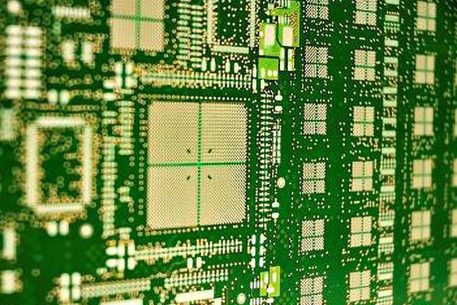
![High Frequency Low Loss PCB manufacturer]()
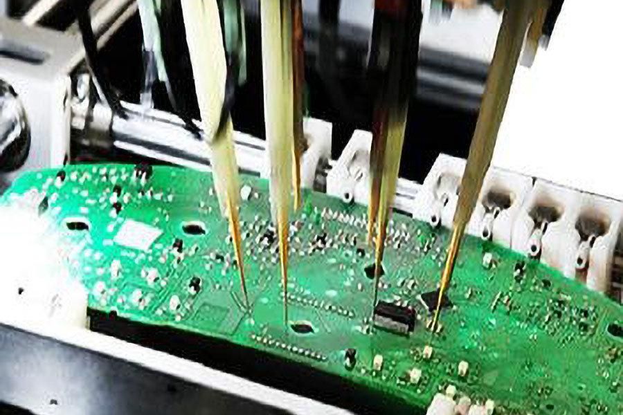
HDI Blind and Buried Microvias PCB manufacturing with High Frequency Low Loss PCB Material, Rigid flex pcb and Flexible circuit
-
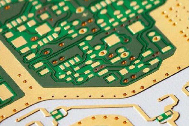
![flex circuit manufacturer]()
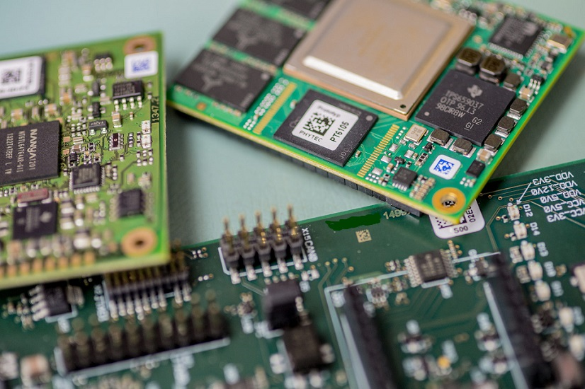
HDI Blind and Buried Microvias PCB manufacturing with High Frequency Low Loss PCB Material, Rigid flex pcb and Flexible circuit
-
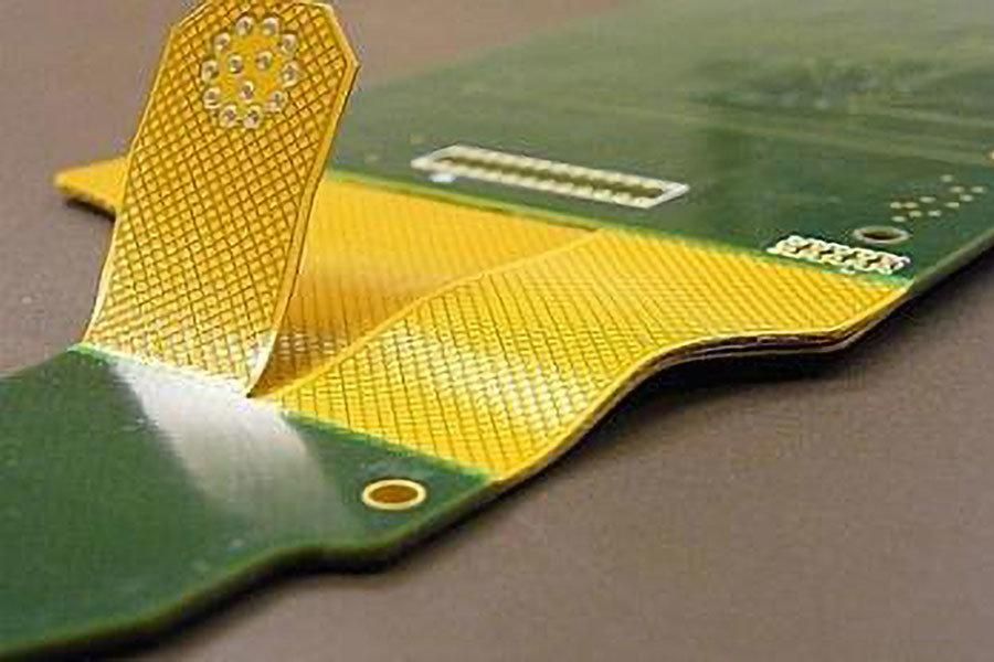
![rigid flex circuit manufacturer]()
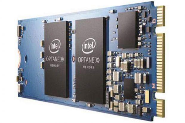
HDI Blind and Buried Microvias PCB manufacturing with High Frequency Low Loss PCB Material, Rigid flex pcb and Flexible circuit
-
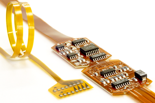
![Turnkey pcb assembly manufacturer]()
HDI Blind and Buried Microvias PCB manufacturing with High Frequency Low Loss PCB Material, Rigid flex pcb and Flexible circuit
-
![RF pcb manufacturer]()
HDI Blind and Buried Microvias PCB manufacturing with High Frequency Low Loss PCB Material, Rigid flex pcb and Flexible circuit
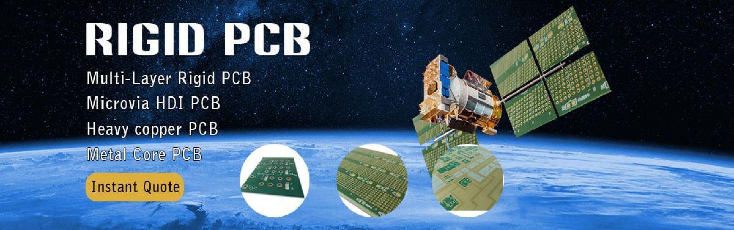

HDI PCB Manufacturing
As a leading PCB manufacturer, Hemeixinpcb offers a full range of rigid board assembly from single / double sided upwards, but it also supports laser drilled microvias, cavity pcb boards, heavy copper up to 30 oz., via-in-pad, microwave & RF PCB boards, up to 58 layers and others.
- Layer count: 2~58L
- HDI PCB, High frequency pcb
- Blind vias / Buried Vias (Mechanical & Laser Drilling)
- Microvias filled by epoxy and copper capped
- Polyimide rigid pcb laminate (Alron85N, Isola P95, Isola P96, Ventec VT901 etc)
- Low loss pcb material (I-Speed material, FR408HR, Megtron4, EM-888, N4000-13EP, N4000-13, TU-863+, TU-872lk, TU-872SLK, TU-872SLK SP etc)
- High Speed Digital PCB laminate: (I-Tera MT40 / RF, Tachyon-100G,Megtron6/R-5775, TU-883, TU-883SP, IT-968, IT968SE etc)
- RF PCB, Microwave pcb laminate: (RO4450F, RO4350B, RO4835, RO4003, RO4533, Taconic TLY series, TLY-5, RF35, TSM-DS3, Astra MT77, RT/Duroid 5880, RO3203, RO3003 etc)
- BGA Pitch down to : 0.15mm (min)
- Min trace width/spacing: 0.002"/0.002"
- Staggered, Stacked and Skipped Microvias HDI: 9+N+9 (any-layer hdi)
- Back drill: Min hole size 15.7mils Depth tolerance +/-6mils
- Cavity PCB Process
High Frequency PCB Manufacturing
Microwave electronics and PCBs operate at signal frequencies ranging from low MHz to very high GHz (mmWave range). These innovative products are built using various synthetic and naturally-occurring materials to ensure consistent operation and signal integrity at high frequencies. Material selection is, in fact, the most critical factor in designing a high-performance microwave PCB.
High frequency PCB materials have certain properties that define their usage for both printed circuits, in interconnect boards, or as standalone assemblies. These include their dielectric constant, thermal expansion coefficient (CTE), and loss tangent or dissipation. In addition to the dielectric material, the copper material used in an RF PCB stackup is important as it will have some roughness, and thus it will determine the skin effect experienced by signals as they propagate along an interconnect.
- Isola High Performance PCB Laminates : (I-Speed material, ASTRA MT77, I-TERA MT40, IS680 AG-348 etc)
- Rogers PCB Materials : (RO3203, RO3206, RO3210, RO4003C, RO4350B, RO4450B, RO4350B etc)
- Arlon Electronic PCB Materials : (AD250C, AD255C, AD260C, AD300C, AD320A, AD350A etc)
- Taconic PCB Materials : (TLY-5, TLC-30, TLC-32, TLF-34, RF-35, TLF-35, RF-60A, TLE-95 etc)
- Panasonic PCB Materials : (MEGTRON 6, MEGTRON 7, MEGTRON 8 etc) for those Networking equipments require an extremely low transmission loss for high Speed communication
- Double-sided process: RT5870、RT5880、RT6010、Ro4360、TMM10、TMM10i
- Hybrid pcb , Blind and Buried Vias; Filled via capability
- Micro Vias Via In Pad with Fill Options (Conductive, Non-Conductive, Copper Plug)
- Tolerance of impedance control: +/-5%
- Special process PCB: Countersink hole pcb, Press fit pcb, Semi flex pcb, Castellated holes pcb, Cavity pcb etc)
- Special Surface PCB: Selective gold plating pcb, Hard gold pcb, Gold fingers pcb, ENEPIG plating PCB
- Back drill: Min hole size 15.7mils Depth tolerance +/-6mils
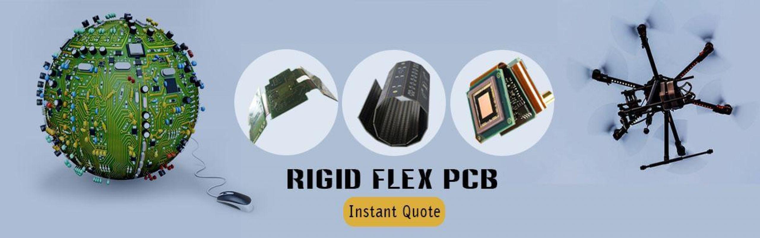
Rigid Flex PCB Manufacturing
Hemeixinpcb can offer the production of rigid-flex and flex PCBs and HDIs for high-reliability applications, with features down to 25 µm and flexible dielectric core down to 25 µm. With the revolution in portable communications products over the last decade, Rigid Flex PCB have become a preferred design solution for complex, three-dimensional product assembly, and advanced component surface mounting demands.
- Blind and Buried Vias (Mechanical & Laser Drilling)
- HDI microvia rigid-flex circuit boards
- Via-In-Pad (Resin Or Copper Paste Filled)
- High frequency rigid flex pcb
- High temperature rigid flex pcb
- Eccobond(Epoxy Strain Relief)
- Cavity Process
- ENIG (Electroless Nickel Immersion Gold)
- ENEPIG (Electroless Nickel Electroless Palladium Immersion Gold)
- Hard nickel/gold
- Wire bondable gold
- Tin
- Organic Solderability Preservative (OSP)
- Silver
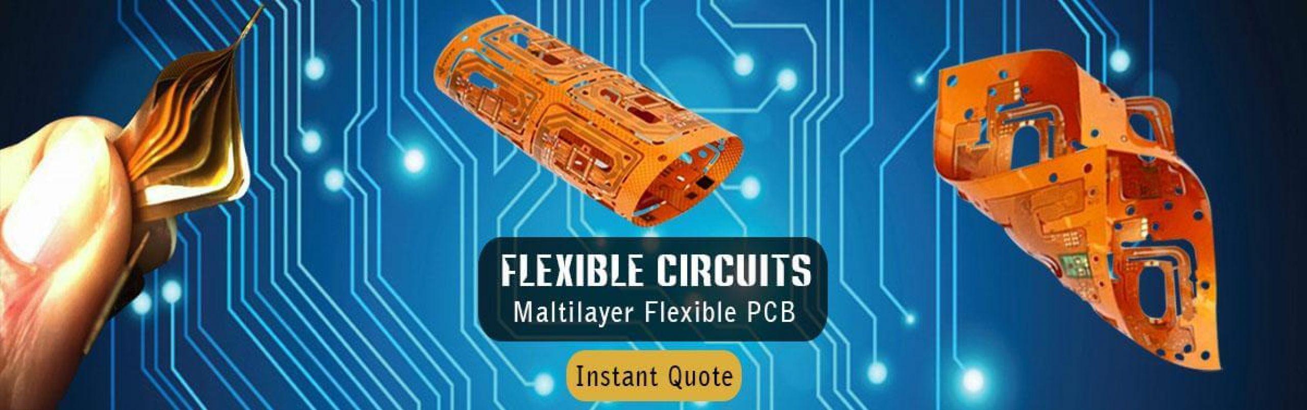
Flexible PCB Fabrication
Hemeixin are committed to meeting your needs for flexible PCBs, whether they’re single or double sided, multilayer, differential copper, jumpers, etc. We offer different substrates such as polyimide (also known by the name Kapton®), PET, PEN, LCP, fibre, and many other innovative solutions. Different thicknesses of copper conductors can be used with surface finishes adapted to your manufacturing needs: assembly of SMT components, frictional contacts, etc.
- Flexible pcb prototype
- Large format pcb
- Long flexible pcb
- High temperature flex pcb
- Single sided flexible PCB
- Double sided flex PCB
- Multilayer flexible PCB
- Thick copper flexible pcb(up to 500 µm)
- Sculptured Flex Circuits
- Immersion silver
- Immersion tin
- ENEPIG: Electroless nickel/electroless palladium/immersion gold
- Immersion nickel/gold
- Electrolytic nickel/gold
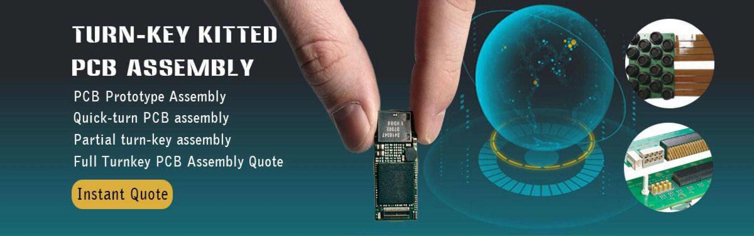
PCB Assembly
Hemeixinpcb is a one-stop shop for all your PCB assembly needs. We provide in-house PCB fabrication, assembly and turnkey services within five days or less.
We specialize in fast turn time prototype and short run PCB Assembly. We use state-of-the-art equipment for our production of reliably assembled PCBs.
- Rigid PCB assembly
- Flex PCB assembly
- Rigid flex PCB assembly
- SMT, through-hole, and mixed technology
- Board sizes up to 20” x 24”
- PBGA, CBGA, TBGA, FPGA, CGA, LGA
- Fine pitch Micro BGA (0.4mm)
- Smallest size down to 01005s
- Prototype PCB Assembly
- Low Volume PCB Assembly
- IC Programming
- Functional Testing
- X-ray Inspection: checks for BGAs, QFN and bare circuit boards.
PCB Prototype
We understand how important it is to have the PCB boards you ordered reach PCB assembly ASAP. That's why we've made every effort to strengthen our core competencies, honing our PCB production capabilities to ensure that we meet your order schedule in the shortest possible time.
Not only do we know the importance of ensuring quick turnaround for the success of your project, but we also know that the resulting quality is equally as important. With our integrated in-house facility, 687-strong workforce, 87+ dedicated team of engineers, 42 different PCB manufacturing stations, and 24/5 production schedule, we can fulfill all PCB prototype assembly projects on tight deadlines faster than the average lead times most PCB service companies can achieve - and with quality, of course. This means the shortest turnaround times and the highest quality for any HDI project as well.
- Quick Turn PCB Fabrication
- High Temperature PCB
- High Frequency PCB
- Flexible PCB
- Rigid flex PCB
- Rogers PCB
- PTFE PCB
- Metal Core PCB
- RF Printed Circuit Board
- High Speed Signal PCB
- Heavy Copper PCB
- Hybrid PCB
- ATE PCB
- BGA Assembly
- Prototype PCB Assembly
- Quick Turn PCB Assembly
- Consigned PCB Assembly
- Complete Turnkey PCB Assembly
Prototype PCB Fabrication Services
Hemeixin builds your Small Quantity boards using the same top-quality equipment, materials and processes that are used to produce production PCBs. Your quick turn, Small Quantity boards are built to your specifications - to meet the requirements that you may have for a fully functional pcb boards for testing or design verification.
| Layers | Standard Delivery | Fast Delivery | Express Delivery |
|---|---|---|---|
| 2 | 5 days | 3 days | 1 day |
| 4 | 6 days | 4 days | 2 days |
| 6 | 7 days | 5 days | 3 days |
| 8 | 8 days | 6 days | 3 days |
| 10 | 10 days | 7 days | 4 days |
| 12 | 12 days | 7 days | 5 days |
| 14 | 12 days | 8 days | 5 days |
| 16 | 13 days | 8 days | 5 days |
| 18 | 14 days | 10 days | 6 days |
| 20 | 15 days | 10 days | 6 days |
Since China’s New Year is approaching, we'd like to inform you that we'll have 5-day holiday from Jan. 21st to Jan. 25th (GMT+8) during which your question or email may not be replied immediately. However, Microvia HDI PCB, RF PCB, Rigid-Flex PCB, Flex PCB quotation or orders can be submitted online or email to us as usual.
In order not to get your manufacturing efficiency reduced, we strongly suggest you submit quotation or order in advance so that manufacturing can be done or started at least before our public holiday. Thank you for your understanding and patience.
Our PCB factory workers start holiday earlier (13th Jan). For bare PCB orders, please kindly calculate the lead date before you place the order. Some boards cannot be finished before our holiday and will be delayed to February.
Together we can plan the best solution for your needs!
Our teams are well prepared to help you put your requests into action and answer any questions you may have.
Do not hesitate to contact Hemeixin for further information about lead time and recommendations for your order planning.
Contact: This email address is being protected from spambots. You need JavaScript enabled to view it.
Send us your PCB, Rigid flex PCB, flexible circuit data files and we will run a complete DFM check for manufacturability. Experience how our engineering support gives customers the most in-depth feedback, with exact accuracy, eliminating delays and quality problems discovered before fabrication. We will check below items carefully.
- Drill Checks
- Solder Mask Checks
- Silkscreen Checks
- Controlled Impedance Checks
- Stackup Checks
- HDI PCB via holes Structures
At some level of circuit complexity, turning to an architecture with blind and buried vias will result in better yield and lower cost than would a through-hole design. Learn more from How to BGA Fanout Routing in your HDI PCB and HDI PCB design guidelines
Sometimes, you can’t fit all your connections on one layer. This is where vias come to your rescue!
Vias are barrel shaped vertical conductive holes that make connections between multiple layers of a PCB. The IPC defines eight different types of vias, but we’re going to talk about blind and buried vias; the two you’re most likely to work with.
A blind via connects an outer layer of the board to inner layers and doesn’t go through the entire board. A buried via connects inner layers without reaching the outer layers. And a through hole via goes all the way through, from top to bottom, connecting all layers.

Fitting More on Smaller Boards
Blind and buried vias provide electrical connections from the outer layers to the inner layers as well as in between the inner layers, and are used when you have limited space on your PCB. Buried vias are hidden beneath the layers and free up surface space without impacting the traces or surface components on the top or bottom layers. Blind vias also free up space, can be essential for fine pitch BGA components and have the added benefit of helping reduce signal stubs through the drilling process as the via terminates at the last connected layer.
You mostly see blind and buried vias in High density interconnect (HDI) PCBs. HDIs provide benefits such as increased layer density, improved power delivery and use of much smaller pitch devices. The hidden vias help keep the board light and compact. It is common to see blind and buried vias in electronic products like, cell phones, laptops, and medical devices to name a few.
Incorporating blind vias and buried vias make more connections and higher board density possible. But not without drawback. Vias add extra steps to manufacturing and testing, which come with added costs.


