PCB Technology
An overview of the PCB Manufacturing can be found here: Microvia HDI PCB, RF PCB, Rigid-Flex PCB, Flex PCB
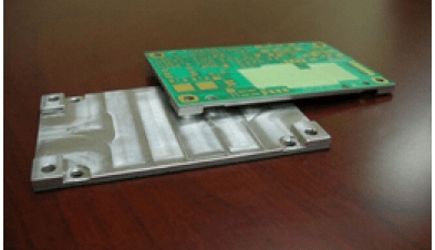
HIGH SPEED DIGITAL PCB Technology
We Always Perform Signal Integrity Analysis for High Speed PCB
The digital circuit is a powerhouse and high-speed PCBs are full of microprocessors and other components that are managing billions and billions of operations each second. That means any flaw or error in design can cause a significant issue and prevent proper operation.
It’s important for any high speed PCB to be properly engineered to reduce flaws through elements such as impedance discontinuities in transmission lines, improper plating of the through-hole interconnections or other losses of PCB signal integrity.
Hemeixin has the experts on-hand to achieve the results you need. We know most digital, high-speed applications have long since risen above the operational efficiencies offered by standard FR-4 materials, so we’ll make the right recommendations and prevent you from having performance issues.
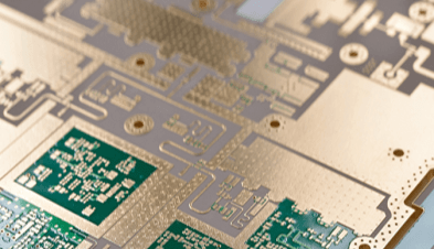
Hybrid PCB and Mixed Dielectric PCB Technology
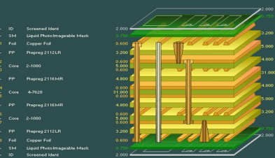
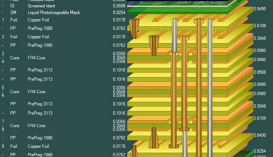
The hybrid PCB stack-up can be used as one of enablers to improve SI for signals routed on selected layers. For a hybrid PCB stack-up, some layers of the PCB use low loss dielectric while the others are fabricated with the traditional FR4. The cost of such a hybrid stack-up is normally lower than all low loss material PCB stack-up, but with the advantage of some routing layers having the same or similar low loss properties as an all low loss stack-up, thus achieving optimized cost-performance. As a contrast to re-driver/re-timer solution which improves SI performance for selected number of links, a hybrid PCB stack'up can improve SI performance for selected routing layers. A hybrid stack-up can also be built by mixing low loss material with ultra-low loss material to further reduce loss in the routing. In short, a hybrid PCB stack-up has the following features:
- Performance improvement over the stack-ups with all standard FR4 board
- Cost reduction over stack-ups with all low-loss/medium-loss board.
There are different options and associated costs for creating a hybrid PCB stack-up. For example, one can use same materials (high loss or low loss) for all the prepreg(PP) layers, and different types of materials for core layers. Another example is to form top and bottom layers as low loss while keeping all other layers FR4, thus having two microstrip routing layers as low loss.
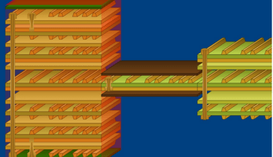
Microstrip in Hybrid PCB Stack-up
For microstrip, a hybrid PCB stack-up has the same performance as all low loss stack-ups, as long as the dielectric of the outer layer is low loss. In other words, if the signals requiring low loss material are only routed on outer layers, the hybrid PCB can get the identical loss performance compared to all-low-loss stack-up, while significantly reduces the material cost.
Stripline in Hybrid PCB Stack-up
The signal may not get full benefit of low loss material unless both sides of the dielectric is low loss material. very often, for stripline in a mixed dielectric PCB stack-up, one side of material is low loss while the other side of material is high loss.For stripline with high loss and low loss dielectric materials on the top and the bottom of the signal layer, the loss is expected to be higher than striplines with same stack-up of all low loss materials on both sides, but lower than striplines with same stack-up using high loss materials on both sides.
Manufacturing capability and the stack-up implementation recipe for a hybrid PCB can differ among PCB manufacturers. The optimal performance-cost solution also depends on the number of signal layers, routing length, material selection, etc. It is necessary to consult your PCB manufacture for the capability and the risk associated such as the yield, de-lamination, etc.
RF and microwave PCB Technology
RF and microwave PCB with high frequency laminates can be difficult to design because of the sensitivity of the signals, especially compared to other digital signals.
Here are a few things to consider that ensure your design is efficient and minimizes the risk of failures, signal disruptions and other intrusions.
- RF and microwave signals are very sensitive to noise — much more sensitive than very high-speed digital signals. That means you’ll need to work to minimize noise, ringing and reflections while treating the whole system with care.
- Return signals take the path of least inductance — ground planes underneath your signal will make it easier to guarantee this path.
- Impedance matching is important. As the RF and microwave frequencies move higher, tolerance becomes smaller. Often, your PCB driver will need to be fixed, such as at 50 ohms, and that means 50 ohms out from the driver, during transmission and sending to the receiver.
- Transmission lines that bend due to routing constraints should use a bend radius that’s at least three-times larger than the center conductor width. This will minimize characteristic impedance.
- Return loss must be minimized, whether it’s caused by signal reflection or ringing. A return path will always be found, but your design should guide it and prevent bleeding of the return through the PCB’s many layers.
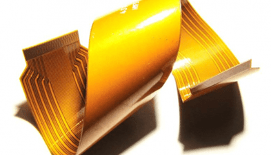
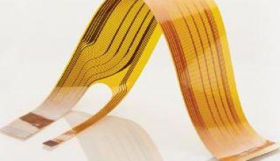
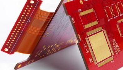
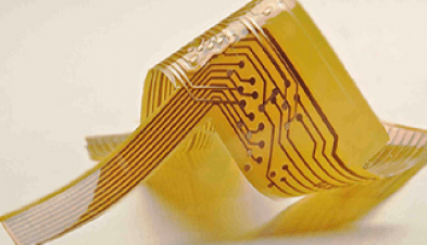
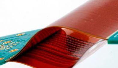
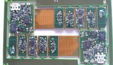
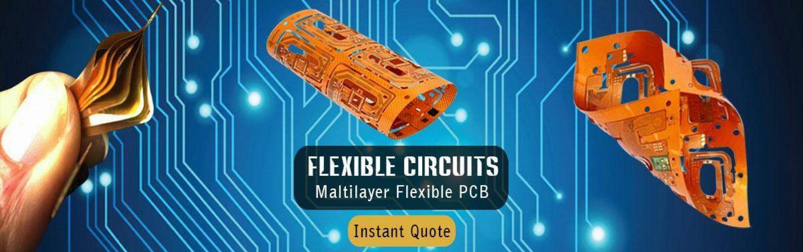
Flex and rigid-flex PCB Technology
Flex and rigid-flex PCB technology offers reduced weight and space savings. Today’s small lightweight consumer electronics are often built with rigid-flex technology, however, there can be many challenges in successful rigid-flex PCB design. Browse our website of pages to learn more about PCBs and rigid-flex design for flexible electronics and wearable designs.
Standard Rigid-Flex provides a cost-effective alternative to rigid Printed Circuit Board (PCB) modules and Flexible Printed Circuit (FPC) interposers/connector systems. Hemeixin integrates conventional plated through-hole, and microvia interconnect processing for intermediate component density designs to give you the best Standard Rigid-Flex solutions. Hemeixin incorporates stiffeners, air gap construction, shielding, and coverlays from our FPC systems as needed.
Hemeixin provides industry-leading HDI capabilities to optimize today's challenging designs. The use of HDI and Every Layer Interconnect (ELIC) stacked copper filled µVias, fine feature etching, and precision registration provide unique, mass-production solutions for complex designs.
With extensive investments in leading-edge production systems, rigid HDI PCB Hemeixin can build the next generation of interconnect solutions.
Rigid-Flex designs utilizing HDI/ELIC capabilities eliminate the need for the module connectors and saves precious space within the slim, high-style designs compact designs. Hemeixin provides this new end-to-end solution from initial design to mass production.
With prequalified materials from our matrix of low-cost, sourced rigid and FPC laminates, coverlays, stiffeners, and shielding, Hemeixin provides end-to-end solutions optimized for cost-sensitive applications. Hemeixin offers engineering support during the design and specification phase, to create an optimal bill of materials and stack-up to deliver low cost, high processing, and assembly yields, and the best reliability.
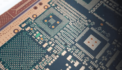
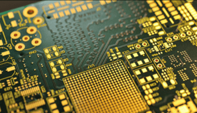
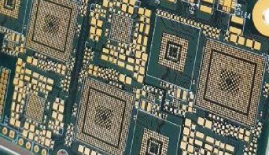
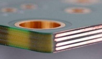
HDI PCB Technology
The processes involved in the production of HDI PCBs are often different than those used with other PCB types. Here’s what you need you know about HDI board production and some of the design considerations you’ll want to keep in mind to keep in mind throughout the production process:
- Sequential Lamination: In the lamination process, the PCB core or cores are combined with copper, as well as pre-preg layers for multi-layer PCBs, by applying heat and pressure. The amount of heat and pressure needed varies from board to board. After the lamination phase is complete, the PCB manufacturer will drill vias. Unlike other types of PCBs, HDI boards go through this process multiple times. These sequential laminations help prevent shifting and breaking during drilling.
- Via-in-Pad Process: The via-in-pad production process allows you to place vias in the surface of the flat lands on your PCB by plating the via, filling it with one of the various fill types, capping it and, finally, plating over it. Via-in-pad is typically a 10- to 12-step process that requires specialized equipment and skilled technicians. Via-in-pad is a smart choice for HDI PCBs because it can simplify thermal management, reduce space requirements and provide one of the shortest ways to bypass capacitors for high-frequency designs.
- Via Fill Types: Via fill types should always match your specific application and PCB requirements. Via fill materials we work with on a regular basis include electrochemical plating, silver-filled, copper-filled, conductive epoxy and nonconductive epoxy. The most common via fill type is nonconductive epoxy. You want to choose a via fill that’s flush with the flat land and will solder entirely, just like traditional lands. Fills must allow microvias and standard vias to be blind, buried or drilled, then plated to hide it beneath SMT lands. We often use multiple drill cycles at precisely controlled depths to ensure the drilling process is done right each time. This level of control requires specialized equipment and longer development time.
- HDI Structures: HDI PCBs come in a few different layout options. Some of the most common are 1-n-1 PCB and 2-n-2 PCB. A 1-n-1 PCB contains a single build-up of high-density interconnected layers, so it’s the “simplest” form of HDI printed circuit board. It requires one sequential lamination on each side of the core. The 2-n-2 PCB has two HDI layers and allows microvias to be staggered or stacked across layers. Complex designs usually incorporate copper-filled stacked microvia structures. Structures can climb to very high X-n-X levels, though complexity and cost typically limit the buildup. Another important option is the any-layer HDI. This involves an extremely dense HDI layout so conductors on any given layer of the PCB can interconnect freely with the laser microvia structures. These designs appear in GPU and CPU chips in smartphones and other mobile devices.
- Laser Drill Technology: Any-layer HDI designs often require laser microvias created with laser drills. These drills generate a laser at up to 20 microns in diameter, which can effortlessly cut through both metal and glass, creating very tiny but clean holes. You can get even smaller holes by using materials such as uniform glass, which has a low dielectric constant.
- LDI and Contact Imagery: Being a leading HDI printed circuit board supplier means pushing the envelope. Hemeixin can deliver finer lines with cutting-edge technology and clean rooms that ensure safe, secure processing. When it comes to these delicate details, repairs aren’t possible, so it must be done right and with extreme precision the first time. We alternate between contact imaging and LDI imagery based on what’s needed for verifying your equipment. LDI is the go-to for fine lines and minute spacing because it can verify even the most demanding processes, continually expanding our capabilities and allowing for smaller form factors.