- Home
- PCB Prototype
- Assembly
- PCB
- Rigid-Flex PCB
- Technology
- PCB Material
- Epoxy Filled Vias
- Heavy copper circuit board
- HDI Micro vias PCB
- Controlled Impedance
- RF & Microwave PCB
- Rigid-Flex Circuit
- Bending And Folding
- Thermally Conductive PCB
- Flex PCB Design Guidelines
- Rigid-flex PCB design guidelines
- HDI PCB design guidelines
- Heavy copper PCB design guidelines
- Flexible PCB design issues
- Flex-Rigid PCB design issues
- Turn-key PCB Assembly design issues
- PCB Trace Width Calculator
- Company
- Quote
PCB Manufacturing Capabilities
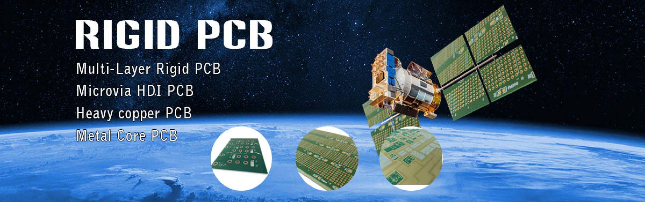
When you work with Hemeixinpcb, you receive our knowledge and experience, resulting in high quality printed circuit boards. Learn more about our HDI pcb and RF PCB capabilities below.
| MANUFACTURING FORMATS | ODB++,HPGL DXF ,Gerber 274X ,Excellon |
|---|---|
| MAXIMUM PANEL SIZE | 48″X 24″(1200mm X 610mm) |
| MAXIMUM THICKNESS | 394 mil(10mm),Samples of 689mil(17.5mm) |
| LAYER COUNT | 2~68 Layer,80+Layer for Samples |
| INTERCONNECT FORMATION TYPES | Back Drilled Blind (laser & mechanical) Dual Diameter Electrically Isolated Thru Hole Buried SMT |
| ASPECT RATIO | 45 : 1 |
| FINISHED HOLE SIZE | 6mil (0.15mm) Mechanical Drill 3mil (0.075mm) Laser Drill |
| BLIND VIA ASPECT RATIO | 1.25 : 1 |
| INTERNAL FEATURES | Inner Layer: 2mil/2mil (Hoz), Outer Layer: 3mil/2mil (Hoz), |
| EXTERNAL FEATURES | Inner Layer: 2mil/2mil (Hoz), Outer Layer: 3mil/3mil (Hoz) Buried Resistors: Dielectric thickness: 14 μm Capacitance /area: 6.4 nF/in2 Breakdown Voltage: >100V 3M material, no need license Buried Capacitance: Resistance (ohms/sq) : 25, 50, 100, 200 |
| MATERIALS | FR-4, Halogen-Free, Rogers, BT, PTFE, PPO, PPE, Polyimide, Hybrid, Bergquist, Arlon, Taconic and etc. |
| COPPER PROCESSING | 20 oz ,30 oz(Sample) |
| IMPEDANCE SINGLE&DIFFERENTIAL | ±10%,±7.5%,±5% |
| VIA FILL | Vias filled with LPI/hole fill mask Non-conductive via fill with epoxy hole fill Conductive via fill with copper paste |
| PRESS FIT | ±2mil(0.05mm) |
| SURFACE FINISHES | Electrolytic Ni/Au (Hard & Soft) ENIG HASL ENIPIG Immersion Silver Immersion Tin Reflowed Tin/Lead OSP |
An overview of the Other rigid PCB Manufacturing can be found here: ATE PCB, rf circuit


- PCB Technology
- PCB Material
- Epoxy Filled Vias
- Heavy copper circuit board
- HDI Micro vias PCB
- Controlled Impedance
- RF & Microwave PCB
- Rigid-Flex Circuit
- Bending And Folding
- Thermally Conductive PCB
- Flex PCB design guidelines
- Rigid flex PCB design guidelines
- HDI PCB design guidelines
- Heavy copper PCB design guidelines
- Flexible PCB design issues
- Flex-Rigid PCB design issues
- Turn-key PCB Assembly design issues
- PCB Trace Width Calculator

Contact us
-
Phone:
-
Email:This email address is being protected from spambots. You need JavaScript enabled to view it.
Copyright © 2024 Hemeixin Electronics Co, Ltd. All Rights Reserved.