
Flex PCB design issues
When ordering flex circuit boards online, quick turn order delivery timelines can incur setbacks if the data set is either incomplete or if the design has technical issues. Technical issues can be related to either manufacturability or the end use of the parts. These issues then often require multiple communications to resolve and in some worst-case scenarios, extensive design revision. Any of these issues will of course delay the delivery of the finished parts.
A successful flexible PCB often depends on two things: the manufacturability of your design, and your relationship (e.g., level of collaboration) with your supplier. Say you’ve decided that flex is the right fit for your application. Already, you have a bevy of additional choices in front of you. Will you go with a single-sided (with or without a stiffener) or multilayer flex PCB, or might a rigid-flex PCB work in this situation? Can your PCB supplier make a board that also meets all of these requirements?
Answering these questions and avoiding costly errors and delays is much easier when you sit down with your supplier and assess the options available to you. Relatively simple designs such as single-layer flex are the most economical, but cost isn’t everything. Make sure the flex PCB you choose is the best technical fit for your use case. Depending on application, a higher manufacturing cost will cut on overall cost in the long run. Pay close attention to the the complexity of the flex PCB application as well as the capabilities and recommendations of your supplier.
In this post we will detail some of the more common flex circuit technical issues we often see that delay quick turn orders to help you avoid delays and complete assembly and delivery of your product as quickly as possible.
1. Flex PCB Board basic specification.
- A part number (including revision number) for your design to ease tracking
- Board thickness (.including flex part thickness and each stiffener area’s thickness).
- Type of board material (Polyimide adhesiveless base material or Polyimide adhesive base material, etc). Polyimide adhesive base material is standard
- Number of layers
- Surface finish (OSP, immersion gold, etc). Immersion gold is standard
- The color for solder mask or coverlay. Yellow coverlay is standard
- Copper weight on outer layer (1 oz., 2 oz., etc). 1 oz. is standard
- Copper weight on inner layers (.5 oz., 1 oz.). Either is standard
- Flex PCB Stiffener material and thickness( FR4, Polyimide, Stainless steel, copper, ect)
- The minimum trace and space widths in your design
- Indicate your board dimensions on a mechanical layer
- Do you want your boards to remain panelized, or supplied individually cut?
- Gerber files, drill files, IPC-356A (optional)
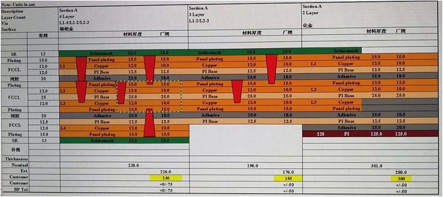
2. Dielectric, Copper weight and solder mask or coverlay requirements on stack up layers are not common to Hemeixinpcb Factory.
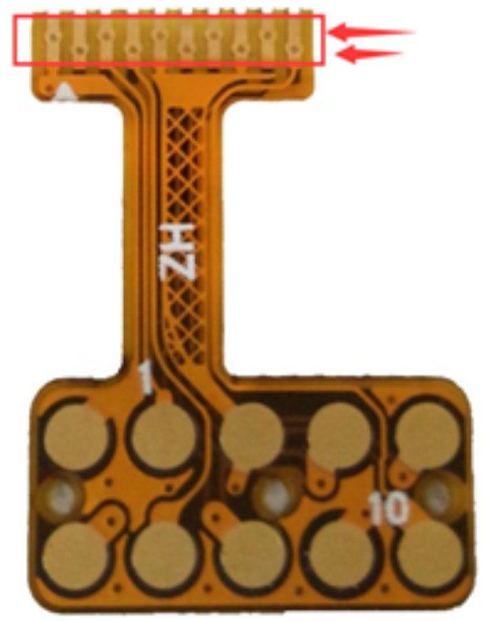
3. Pad to pad distance of less than 27.5 mils is not enough to build coverlay dams in between pads and at the same time ensure there will be no coverlay on pads.
4. Pad to pad distance of less than 10 mils is not enough to build solder mask dams in between pads and at the same time ensure there will be no solder mask on pads.
5. There are vias with soldermask clearance on both sides. But this requirement on flex pcb coverlay is not common to Hemeixinpcb Factory.
6. Via holes on expose pads in parallel.
Holes should not directly “parallel” on each other. Holes in tension (on the outside of the bend radius) may crack when the circuit is bent if they directly align in parallel with a trace on the other holes. The holes in tension are forced farther from the neutral axis of the folded region and can fracture, especially with repeated bending. A good flex pcb design practice is to keep the holes in the neutral axis of a bend by designing this region as a single conductive layer. When this is not possible, a proper design will “stagger” the holes between one hole to the other hole to prevent top and bottom alignment.
Since flex circuit dielectrics are so thin, stitched vias are of questionable value in protecting against EMI. If they are incorporated in a circuit design, they should be kept away from the bend area, as they are discontinuities that can lead to cracks in insulation. Please keep these Plated Through Hole by intricate and Plated through-holes should be kept out of the bend areas
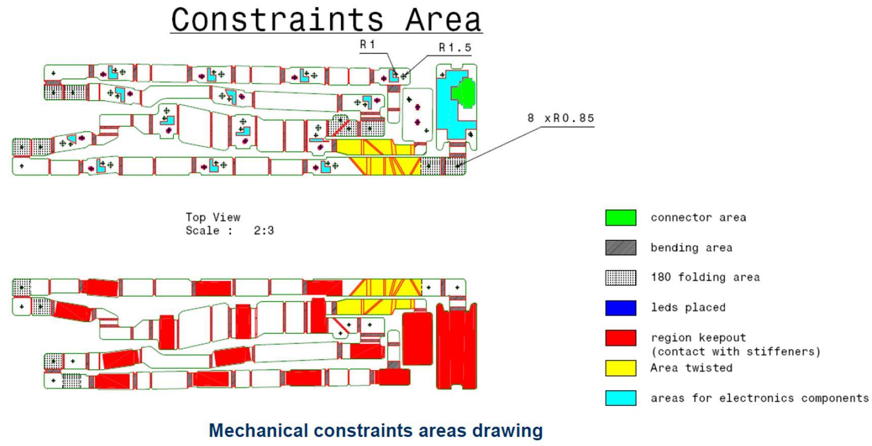
7. No foil weight, Dielectric, coverlay, bending area, stifferents details for flexible circuit is indicated on the stackup and/or drawing notes.
Getting a great flex PCB starts with finding a top-notch PCB supplier like Hemeixinpcb. Check out our main flex PCB page to find out more, and also be sure to take a look at our flex PCB design guide.


