What’s Different About HDI PCB Design and Manufacturing?
The manufacturing process for HDI and regular PCB boards have key differences that are worth exploring.
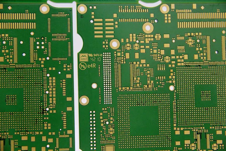
For starters, HDI boards use more layers, smaller microvias, thinner traces, and other components. All these improvements allow HDI boards to be more compact yet functional and compatible with design software.
It is important to leverage automation in design software to get the most out of HDI boards. The exact requirements of HDI boards depend on layer specification and material selection.
The Material Side of Things
Material selection is an important aspect of HDI PCB design and must consider the following questions:
- Adhesion of copper to dielectrics. Most manufacturers require 6lb/in per 1 ounce of copper.
- Compatibility between plated microvias and the dielectric material.
- Chemistry compatibility between the core substrate and dielectric material.
- Is the spacing of the dielectric material between the metal layers adequate and reliable?
- What are the thermal properties of the dielectric material?
- What is the glass transition temperature (Tg) of the dielectric material and will it be sufficient for rework and wire bonding?
- Is the dielectric material capable of surviving extreme temperatures that are usually associated with multiple reflows, solder floats, and thermal cycling.
The dielectric material of choice for building HDI boards are as follows:
- Laser drillable prepegs
- Thermoplastics
- Traditional prepegs and FR4 cores
- Dual layer and reinforced resin coated copper (RCC) foil
- Heat curing of dry films
- Heat treated liquid dielectric
- Polyimide flexible film
- Photosensitive dry film dielectrics
- Photosensitive liquid dielectrics
It is worth noting that most of these materials are not covered by IPC standards.
The design process of HDI boards depends on a carefully thought out plan. There are various aspects of the design that must be considered including:
- HDI stackup
- Via routing and architecture
- Placement of parts
- Design rules
- BGA fanout
The most important aspect of HDI design is the planning of via size, trace width, and BGA placement (as well as escape routing).
It is recommended to contact the manufacturer in order to become acquainted with the fabrication processes for high density interconnect PCB manufacturing. Designers should understand the limitations associated with certain fabrication methods it would have an impact on component placement and layout strategies.
Moreover, via size should be based on the ball pitch design of SMD components. This will have an impact on the manufacturing process for HDI boards.
The most important aspect of HDI PCB design and manufacturing is the use of microvias. There is no room for error when it comes to micro via PCB placement because they will affect overall performance.
HDI PCB Design and Manufacturing Processes
As mentioned earlier, there are similarities between HDI boards and regular PCBs, with major exceptions. HDI boards utilize advanced processes that may not be used with other boards. Let’s take a look at aspects of design that are specific to HDI PCB:
- Contacting the manufacturer to select appropriate materials and use dielectric data for building the best PCB stackup.
- Designers should determine the layer count needed to route all signals. This can be done with the assistance of the biggest SMT device on the HDI board or with the help of interface and direction count from the biggest IC on the PCB.
- Determine via style and placement based on thickness and layer count. The vias are used for signal routing through the inner layers of the dielectric material.
- Conduct a reliability test where needed to ensure that material selection aligns with the assembly process and operation.
- Designing the board based on reliability requirements (such as clearances, trace widths, tear drops, and others) and manufacturer capabilities for assembly and manufacturing.
Stackup design is a critical aspect of HDI boards because it will determine how the circuit will be routed to ensure the product's reliability. Once the designer has covered all the above points, they can follow through with the next steps that are outlined by their design software.
Doing this at an early stage is extremely important and will ensure that the design is routable, manufacturable, and reliable.
Important Design Requirements
Let’s take a look at some of the most important design requirements that are crucial for HDI PCB performance:
- Spacing limits and trace width
- Adhering required aspect ratios when reliability is important
- Impedance profile of the materials and multilayers
The design tools you use when working with your HDI circuit will play a role in meeting manufacturing requirements. It would be relatively easy to control impedance with the help of appropriate design tools.
All you need to do is configure the impedance profile of the material used in the circuit while aligned with the required trace width. Design software such as DRC engines in the routing software can be used to check the routing as you work your way through the HDI layout.
Ask your designer to provide you with the detailed specifications to ensure you have considered all aspects of design and manufacturing.
HDI Via Formation
It is not recommended to use mechanical drilling for via formation in HDI PCBs because their interconnects are smaller than 6 mils. Via in pad design is an alternative method of placing vias in the copper landing of HDI PCBs.
Via in pad design is used to increase density and is an easy way of adding more components into the design because they facilitate a direct connection to the internal layers of the board.
Although larger vias can be drilled, they are more expensive in the long run compared to laser drilling. Mechanical drilling also has a lower throughput because of the slower drilling speed. Laser drilling is the go-to solution for microvia hole formation in HDI PCBs. If speed is an issue, designers can utilize chemical etching of small vias with a speed of more than 10,000 vias per second. Other methods of via formation include photo via formation and plasma via formation.
Are you looking for cutting-edge solutions in HDI PCB design and manufacturing? Get in touch with the experts at Hemeixin PCB here.


