PCB prototype
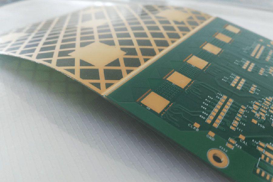
We got a PCB prototype inquiry from the US that requires high volume 8 layer 1.0mm PCB, OSP + selective ENIG surface, 5 groups impedance control, and stacked vias. These requirements are common, but there are 2/2mil lines in inner layers. It’s said that this PCB prototype order was produced at Foxconn. Any PCB prototype manufacturer can do it?
I think most manufacturers can not make this PCB board with a 2/2mil line in high volume since the bad rate is high. But anyway you can share your Gerber files to some professional HDI PCB prototype manufacturers, like email to This email address is being protected from spambots. You need JavaScript enabled to view it.
it’s said that Hemeixinpcb is trying to manufacture this PCB prototypes to check whether they can put it into mass production.
These HDI PCB prototypes have succeeded yesterday. I’m proud I have a chance to review the working Gerber in the MI department. Hemeixinpcb proved their processing capacity and confirmed they can manufacture this 4+n+4 PCB in high volume.
- 18 groups controlled impedance with single-sided and diff.
- 1.8, 2.1, 2.2, 2.3, 2.5, 2.6, 3.0 mil lines in inner &outer.
- 8 BGA with via-in-pad.
- staggered vias, blind vias & buried vias.


