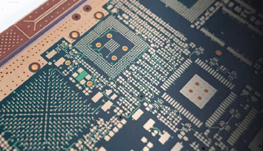
Epoxy Filled Vias
The use of via-in-pad technology is expanding quickly in today’s printed circuit board designs. The requirement for scaling down joined with the quickly diminishing pitch of segment impressions, drives printed circuit board designers here. Via-in-pad requires the vias to be filled, planarized and then over-plated with copper. Regularly, these vias are loaded with either Epoxy Filled Vias, conductive epoxy or strong copper plating. All have upsides and downsides to being considered. By means of Fill is an uncommon PCB producing procedure used to specifically and totally close through openings with epoxy. There are numerous cases in which a PCB planner should need to have a by means of filling. Filling of plated through openings isn’t new to the PCB creation industry.
For a long time, end clients required a few or all by means of gaps to be halfway stopped with weld veil. This undertaking was required with a specific end goal to keep weld from wicking through the holes (to the component side) amid the assembly process and to make a vacuum for electrical test. Limiting motion buildups in the openings is another substantial motivation to attempt this activity. Non-Conductive of fill still has copper plated vias to lead power. The through, regardless, is stacked with an exceptional low shrinkage epoxy phenomenally figured for this application. Conductive methods for fill has silver of copper particles flowed all through the epoxy to give extra electrical conductivity.
A plate-close process gives more noticeable unfaltering quality to little scale through, rather than stacking with non-conductive ink and after that plating over. Filling vias makes a solid focus. This considers a level surface to be plated keeping the fix at the get-together level from spilling through and haggling the dilemma joint. This suits the most trustworthy finished gathering. Come on offers an assortment of printed circuit board fabricating answers for Plug Via Process necessities. Filled by means of in cushion is an approach to accomplish the middle of the road thickness with a halfway cost contrasted with utilizing blind/covered vias.
Want to know more information about Epoxy Filled Vias circuit board log in to https://www.hemeixinpcb.com/ or you can mail us through our mail at: This email address is being protected from spambots. You need JavaScript enabled to view it.


