High Density Interconnect PCB Technology
Today’s high density interconnect (HDI) printed circuit boards (PCBs) increase the functionality of a circuit board while taking up less area, driven by the miniaturization of components and IC substrate packages. It enables an increasing number of advanced features in today’s mobile and high-performance devices. As the pin count of substrate packages increases, and/or the pitch count decreases, HDI PCB structures is a solution to the very complex routing requirements of these devices. Dow Electronic Materials continues to innovate by enhancing Cu via fill chemicals that are essential to building HDI PCB boards.
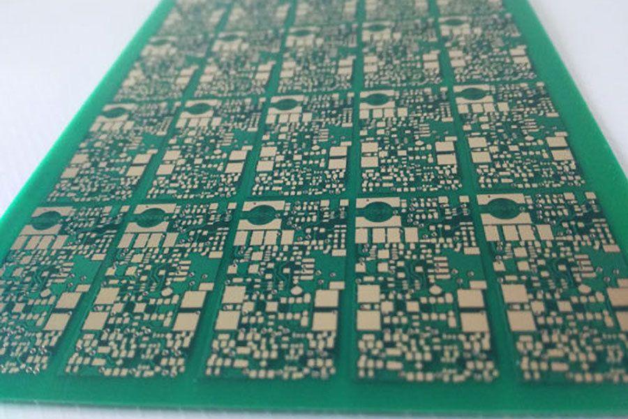
- HDI PCB is defined as a PCB with a higher wiring density per unit area than a common PCB.
- HDI PCB has finer lines and spaces, is made through Micro Via (< 150um diameter)
and buried vias, sequential lamination with insulation materials and conductor
wiring for a higher density of routing.
Compared to standard multilayer PCBs, High-Density Interconnect (HDI) printed circuit boards feature finer conductive path structures and smaller vias. This is the technological response of the HDI PCB industry to permanent miniaturization that requires more and more complex circuits and components with extremely high pin count.
Laminating more HDI PCB layers in Sequential Build Up (SBU) technology enables interconnection and routing of inner layers without consuming surface area, which can thus be used to place and interconnect high pin count components.


