
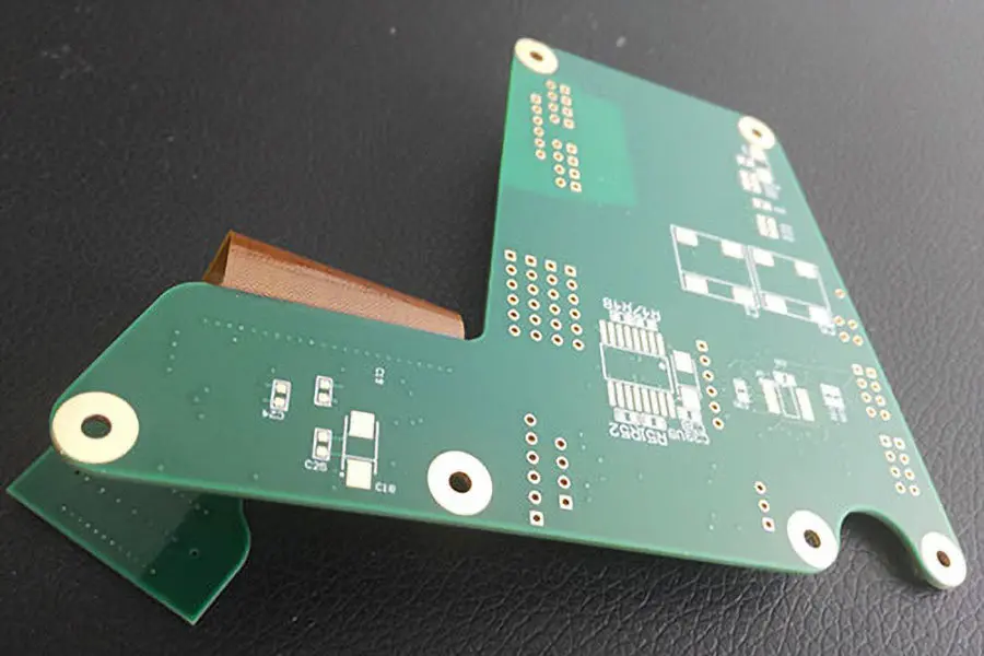
Development and application of Heavy Copper Printed Circuit Boards – PCB Manufacturing Capabilities
The Heavy Copper PCB – PCB Manufacturing Capabilities, has reformed the electronics business. Designed in the year 1930, it has come to be utilized as a part of each believable electronic gadget. This article clarifies the significance of these boards and inspects their advantages and manufacturing choices.
Why Use A Heavy Copper PCB – PCB Manufacturing Capabilities? What Can It Be Used For?
Before going into more details, it’s imperative for you to know the possible utilization of Printed circuit boards, and why you should utilize them (i.e., what their favorable circumstances are).
What would you be able to utilize them for? Completely like everything! There’s mainly no electronic gadget that can’t be constructed utilizing Heavy Copper Printed Circuit Boards – PCB Manufacturing Capabilities. Aircraft, automobiles, computers, TVs, music players, cell phones, Battery-operated toys – nearly everything that uses a type of electronics, make utilization of them. Regardless of whether you’re a hobbyist building a toy, an understudy doing science-extend, or an apparatus producer manufacturing a massive number of gadgets, the utilization of printed boards offer advantages.
Firstly, a Heavy Copper Printed Circuit Boards – PCB Manufacturing Capabilities is considerably littler than different sorts of circuits. Its decreased size is a critical perspective to its general production process. What’s more, a printed circuit significantly lessens the requirement for wires. This improves the presence of the last circuit and enhances durability. For mass-makers requesting in massive production, it’s the least expensive method, offering huge money-saving advantages.
What are the Key Design Considerations when making a PCB?
There Are Three Main Elements:
- A cover board.
- The components mounted on the board.
- Traces that fill in as the “wires” connecting parts and framing the circuit.
The genuine parts utilized depend altogether on the reason for the circuit. Analyzing which components to use is best managed in an encyclopedia arrangement. This leaves laminate boards and traces. The production costs, working proficiency and working expense of the finished circuit, all rely upon these components.
Heavy Copper Printed Circuit Boards – PCB Manufacturing Capabilities is the most ordinarily utilized material for traces. Basic techniques include plating the whole Heavy Copper Printed Circuit Boards – PCB Manufacturing Capabilities, and after those etching away unnecessary regions through a mask (stencil) to leave the needed traces. More complex techniques enable traces to be included in an open board. Each approach has related advantages and disadvantages. A few boards require the utilization of gold for sensitive,
low-voltage applications or (RoHS) consistency. Copper traces typically demand the utilization of a nickel obstruction layer before gold-plating. This is to keep gold from moving into the copper. Unpredictable usage of nickel can bring about the loss of impedance. If you need to build up a custom PCB, it’s suggested that you initially spend little time understanding the nuts and bolts of Heavy Copper Printed Circuit Boards – PCB Manufacturing Capabilities design. There are a few nitty-gritty aides and tutorials. Additionally, plan and simulation software are accessible to enable you to test your outline before you make a heavy copper PCB Prototype.


