Reduce Your PCB Costs with Blind Vias, Buried Vias and Microvias
Printed Circuit Boards (PCB) have come a long way in a short while, but they are still being developed and evolved. PCB fabricators and designers are constantly working to enhance the efficiency, reliability, and ruggedness of circuits while keeping the manufacturing cost down as much as they can. Considering the complexity of the modern circuits and the necessity for more and more compact circuits, reducing the cost is not an easy task. But there are ways to keep your PCB cost to a manageable level, with the help of blind vias, buried vias, and microvias.
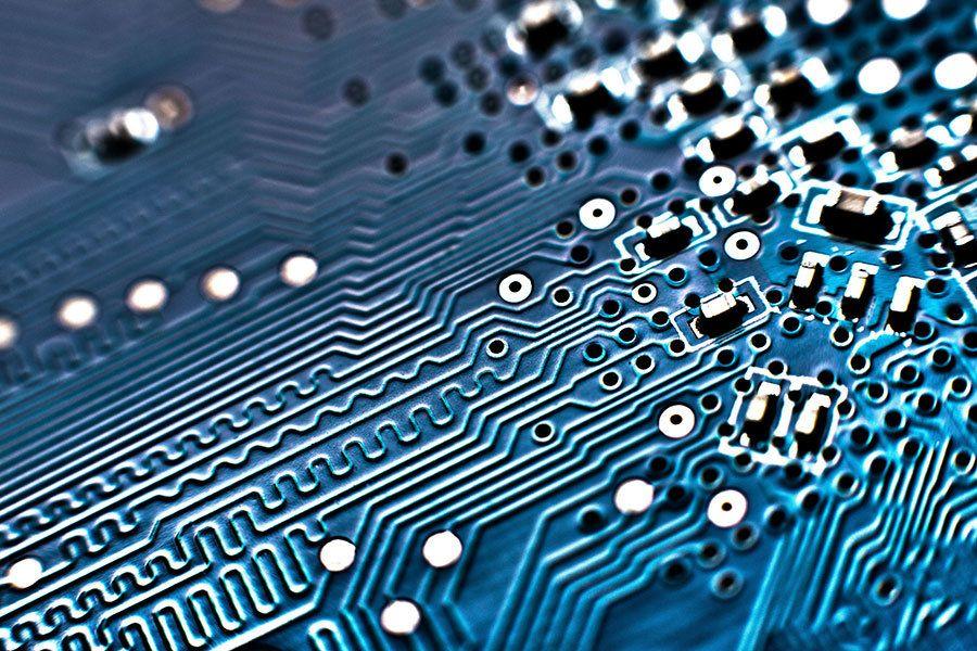
Blind Via, Buried Via, and Microvia
The most common type of via has always been the Plated-Through-Hole (PTH) via. As the name suggests, a PTH via goes from the top to the bottom layer of a PCB. It can also be called a surface-to-surface via. The word Plated refers to the conductive metal plating that goes from the top to the bottom of the hole, making an electrical connection.
A blind via is different. It is from the surface to an inner layer. Most blind vias only penetrate through to the first layer, connecting it to the surface. But blind vias can reach an inner layer further down the sequence. Blind vias are only visible from one side of the board, i.e., the surface they start from. Buried vias, on the other hand, are not visible at all. They connect the inner layers of the PCB. This is why there cannot be buried vias in PCB with less than four layers. Microvias are laser-drilled holes that form the core of HDI technology. Microvias can be blind as well as buried.
The efficiency and design freedom provided by buried, blind, and micro vias are some of the reasons why PTHs are rapidly becoming a thing of the past, especially since most of the components that require PTHs to be mounted on a PCB are bulky and space-consuming. And they make the assembly process a lot harder. PTH technology is now giving way to SMT that allows the overall circuit to be much more efficient and compact. This is one of the reasons why blind, buried, and micro vias are becoming more and more common.
Blind Via
Blind vias can help reduce the cost by allowing more traces on the PCB surface. Let’s say you have five PTHs with only two traces possible between two adjacent PTH. Between the five of them, there would be eight traces running on either surface. If you replace just one PTH with a blind via, the space you saved will allow for two more traces. That’s a 25% increase in the number of traces on one surface.
An increased number of traces will help you keep your layer count down and the board size to a minimum, reducing the overall cost.
Buried Via
Buried vias provide an even more superior level of space-saving on the surface and, consequently, compacting the overall PCB even more. Since buried vias are only placed between internal layers, they allow more space for traces and pads on both outer surfaces. This reduces the overall PCB cost by efficient use of space.
Another way buried vias can help reduce PCB costs is by maintaining the aspect ratio. An aspect ratio of more than 10 or 12 usually incurs an extra cost. Even though with mechanical drilling, the diameter is more important than the aspect ratio, the aspect ratio still needs to be considered for PCBs with smaller BGA pitch requirements. Some fabricators do allow aspect ratios as high as 26 for special cases, but there would be no avoiding the cost.
Buried vias don’t need to break out to the surface while they make connections between the traces of two layers. It allows the traces to mimic a coaxial cable, replicating its characteristic AC impedance. This controlled impedance tracing is something that PTHs don’t allow.
A functional impedance controlled design using only PTH would be very costly. It will require expensive components and a complicated design. This unnecessary cost can be eliminated using buried vias.
Microvia
Microvia is the core element of an HDI design. These laser-drilled vias are what allowed PCBs to shrink. HDI circuits have a higher pin density and more traces, which allow the components to be packed in a compact circuit. In general, microvias reduce a lot of tooling and drilling costs that you would have paid for mechanical drilling. If you are only working with PTHs, the drilling costs alone can easily reach up to about 40% of your total PCB fabrication cost; depending upon the number of holes that were drilled.
Mechanical drill bits have severe limitations regarding the diameter holes as well, affecting the aspect ratio. This is not a problem with the laser-drilled microvia, which can drill holes with diameters as low as 50 mm. And since laser drills don’t suffer from the mechanical tear-and-shear, there is no high tooling cost. Although the number of holes still mater in cost consideration because many buried and blind microvias need to be filled with epoxy or a conductive material.
Microvias can drastically reduce the number of layers needed in a PCB, saving a lot of cost in the process. An eight-layer PCB with PTHs and mechanically drilled blind and buried vias can be shrunk down to 4 layers with microvias. A very simple way microvias save space is with smaller pad sizes. Very small pad diameters allow the trace widths to be maximized. Microvias also help ease the BGA breakout. It’s only because of microvias the BGA breakout pitches can be as small as 0.4 mm (15.7 mils).
Microvias are usually drilled per layer, maintain an spect ratio of 1:1. But more microvias can be stacked on top of each other or staggered (more cost-effective) to connect to multiple layers, or even top and bottom surfaces.
Microvias also help reduce cost by eliminating the need for costly components that are necessary whenever PTHs are used in a high-frequency circuit. PTHs usually cause discontinuities when the frequencies traveling through the circuit reach up to gigahertz, which is very common these days. If a high-frequency circuit is designed using only PTH, an expensive high-frequency material will have to be used as a substrate instead of normal FR4. A series of buried and blind microvias can help eliminate this need, which helps save a lot of money.
Conclusion
PTHs transformed the technology in their time, just like blind vias, buried vias, and microvias are doing right now. These technologies are still evolving, and soon, they might become as cost-friendly as PTHs. Microvias are relatively costly for simpler designs, but for more sophisticated PCBs and prototypes, they are the prime solution.
We offer microvias and pad diameters as low as 50 micrometers and 150 micrometers, respectively. When you are designing your HDI pcb with a layer count as high as 68, you will appreciate the very thin dielectrics of 50 micrometers. Along with buried microvias, a thin dielectric will help you keep the thickness of your circuit in check, and consequently, your aspect ratio.
For cost consideration or better performance, you might want to experiment with different via shapes. With our mechanical and laser drills, we can drill straight-walled, positive and negative tapers, and, cups among others. We are committed to delivering you the highest quality at most reasonable prices. And we will work with you in reducing the overall cost of your circuit as much as we can.


