What Is HDI Substrate?
Printed circuit boards are the foundation upon which electrical appliances are built. They involve ever-changing technologies and designs to cope with the increasing complexity of modern products.
As a result, PCB designs have undergone significant changes. Some readily used printed circuit board designs represent categories, such as rigid boards, flex boards, rigid-flex boards, and HDI printed circuit boards.
HDI or high-density-interconnect circuit boards are making waves in the global market among the common types of PCBs. In this article, we will explore what they are and the types of HDI PCB substrate being used.
What Is HDI PCB?
HDI printed circuit boards are based on a design model that offers higher wiring density compared to traditional PCBs. It offers enhanced electrical output and performance by handling larger electrical loads.
Therefore, HDI PCBs use a number of technologies that allow them to function in the required manner. They use smaller vias, refined lines, and copper traces and offer higher connection pad density. HDI printed circuit boards are gradually growing in popularity since modern electrical applications are more focused on reduced size and increased electrical performance.
As a result, HDI printed circuit boards are designed to be compact, lightweight, have a low layer count, and offer high wiring density, which allows designers to utilize just one HDI PCB instead of using a large number of traditional boards to meet their electrical requirements.
Types of HDI PCB Substrate Technology
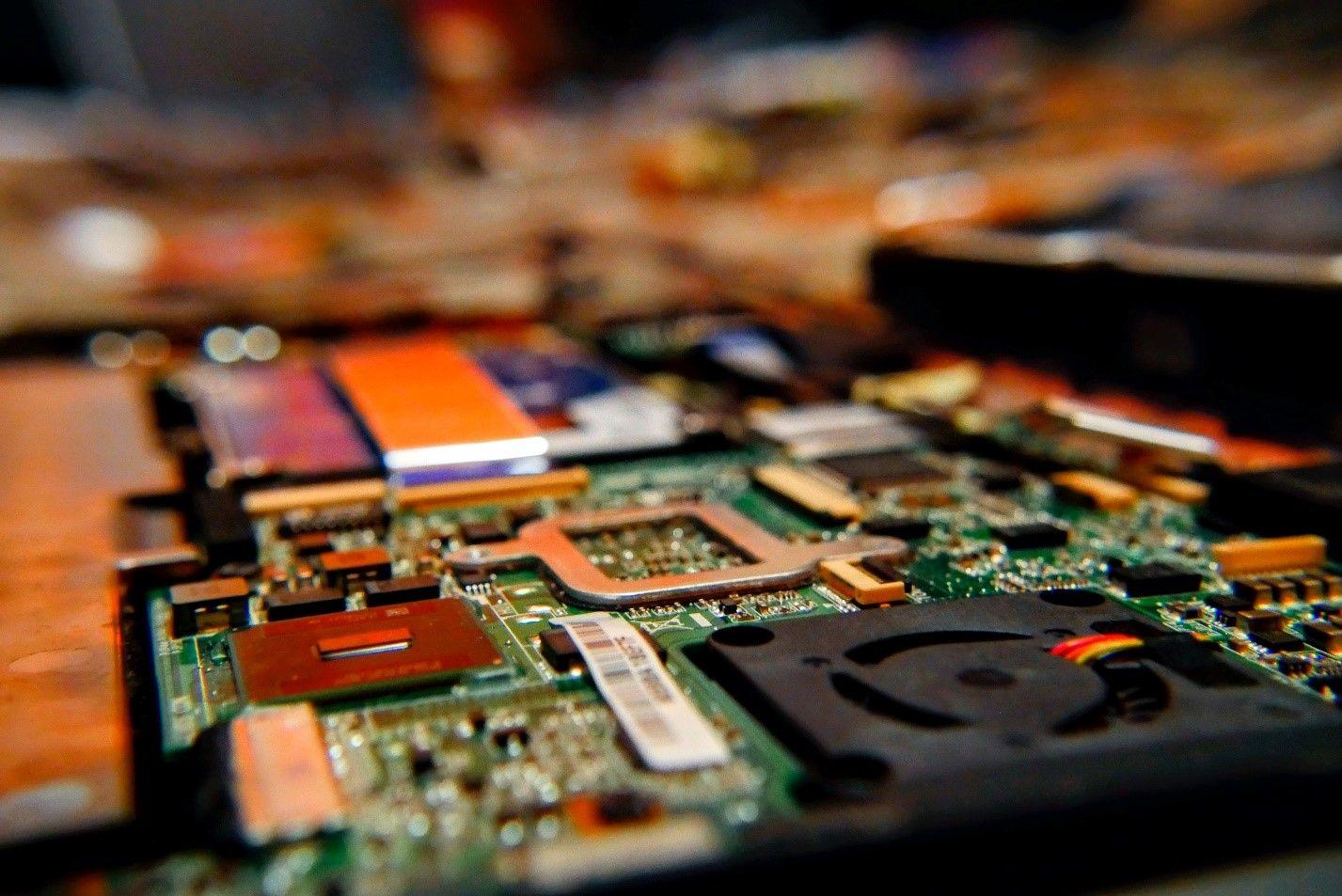
A substrate is the physical foundation that holds the components and traces of a printed circuit board. HDI substrates comprise multilayered, high-density circuits with refined lines and space patterns, increasing their functionality while using less space.
The multiple layers of HDI printed circuit boards have copper-filled microvias that allow for vertical interconnections between the layers. This allows for free signaling between the layers as the current can pass through the microvias, which are typically 150 microns or less in diameter.
Many types of HDI substrate technology have evolved based on the fundamental miniaturization of components and the development of increased functionality.
Moreover, the types of HDI substrate technology involve the utilization of different HDI stack-ups and the types of microvias technology.
Types of HDI PCB Vias Technology
Vias are tiny conductive holes that are the reason for HDI PCBs offering increased functionality. The different types of via technology in HDI substrate depend on the application and design requirements. Let’s look at the following types:
i. Through-Hole Vias
This via technology is simple and cost-effective as compared to the other types. Through-hole vias are generally divided into two broad types: Non-Plated Through-Hole Vias and Plated Through-Hole Vias.
Plated Through-Holes involve the use of copper pads for increased conductivity. The holes are either laser-cut or made using a drill to connect all the HDI printed circuit board layers.
ii. Buried Vias
Buried vias are located inside the PCB structure and are not visible from the outside, hence the name, “Buried Vias.” It is recommended to use an even number of layers for the buried route. A separate electroplated hole is also drilled in the buried through.
iii. Microvias
Microvias are the smallest type of vias technology and also the most popular since they offer optimal performance and high circuity density while maintaining a small size. These are laser-cut vias with a diameter of 150 microns or less. They are used to connect the many layers of an HDI printed circuit board, and their small design helps designers connect dense PCBs to single layers more easily.
iv. Blind Vias
Blind vias are drilled from the external region of a printed circuit board to the inside. The design makes the hole visible from only one side. Both blind and buried vias involve the use of via fill material and special equipment, such as conductive or non-conductive epoxy filling, silver filled, copper filled, and electrochemical plating.
Therefore, these designs can be costly and time-consuming to fabricate.
Other popular advanced features utilized in HDI printed circuit boards include stacked vias, staggered vias, and via-in-pad technologies to maximize space utilization and increase functional aspects.
Types of HDI PCB Substrate Fabrication
The types of HDI PCB substrate fabrication technology and designs have also seen a drastic change with the help of improving via technology. These were some of the most used designs over the course of the last decade, displayed in descending order:
• Build-up
• Sequential Build-up
• Stack-up Via
• Filled Through-Hole
• Filled High AR Hole and Vias
Similarly, the fabrication process has also undergone a revolution, shifting from the conventional subtractive process to a semi-additive process more focused on laser-cut vias, thin copper traces, and improved etching technology.
Microvias are an important part of new generation HDI substrate technology since they allow for better product miniaturization and improved performance. They require the use of electroplating additives, such as electroplating levelers and suppressors, to the HDI substrate for copper electrodeposition. Electroplating additives help with thin surface deposition and smaller dimples.
Additionally, additives are also required for improving etching technology which is required for better space pattern style and refined lines. Etching additives help in the design of HDI printed circuit boards with enhanced etching inhibition at channel sidewalls, high aspect ratio etching channels, and overall finer circuitry.
Since the demand for HDI printed circuit boards is growing, more companies have started manufacturing HDI PCBs for high-tech applications, but since the fabrication process requires specialized equipment and capacity of advanced features, many manufacturers cannot satisfy clients.
Visit Hemeixin Electronics to get custom-built microvias, HDI printed circuit boards, and many other types. They are at the forefront of circuit board innovation and are one of the leading manufacturers of HDI printed circuit boards.
Moreover, they are experts in circuit board fabrication processes, developing highly miniaturized components, equipment, and thin materials for use in circuitry. Hemeixinpcb offers high-quality and precise designs for clients with their Automated Optical Inspection (AOI) technology for defect detection. Visit their website and get a quote today! We hope you now know the importance of HDI PCBs and the types of HDI substrate.


