How to reduce HDI PCB cost
At some level of circuit complexity, turning to an HDI architecture with blind and buried vias will result in better yield and lower cost than would a through-hole design. In
this article, we discuss several design examples and illustrate the relative costs and benefits of different architectural approaches.
Today, we will be discussing manufacturing and cost considerations for your HDI PCB. More specifically, the key things to remember when designing your high-density interconnect board - or HDI.

1. Keep Your Cost Down
One of the problems designers face is keeping cost down. My goal is to provide some insight to help you with your decision-making process. So let’s dive right in! When making PCB-design decisions for HDI, one of the primary concerns is in regards to manufacturability and cost. Just like standard PCB designs, HDI PCB boards have four main concerns: HDI PCB materials, layers and laminations, vias in HDI classes, and optimal trace and space.
Let’s start with materials. Materials play a large role in terms of manufacturability and direct cost of your circuit board. Here is a tip: The goal is always to select the right material for manufacturability that, at the same time, meets your temperature, and your electrical requirements. When it comes to materials, make sure that your high-speed material is also suitable for your HDI PCB design. They are many other factors that come into play when selecting the proper materials for your design.
When thinking about layers and laminations, keep in mind the following questions: Have you planned your layer sequencing for reduced EMI? Have you decided your routing density?
What is the total number of sequential laminations? And have you minimized your laminations?
2. Via Structure
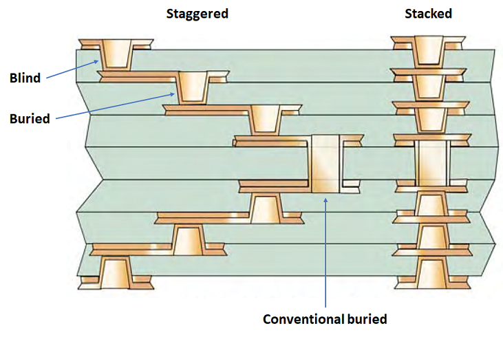
Let's move on to vias. Manufacturability primarily has to do with via structure. Answer the following questions before you start working on your next project: Are you meeting the design guidelines for microvia aspect ratio? Are you stacking or staggering your microvias?
And lastly, trace and space. Have you considered reducing your trace width to increase density and ultimately reduce your layer count? Here is a brief plug on Hemeixin: If you are considering reducing your trace width to increase density and reduce your layer count, 2 mil trace and space may be exactly what you are looking for. Our yields are 90% for this density. When it comes to the manufacturability and the cost of an HDI PCB board, it is very important to remember that none of these considerations can be dealt with in isolation. For example, reducing your trace and space will always ultimately reduce your layer count Or how can you plan your via and pad sizes which impact the space you have to route your traces?
3. Complexity Equals More Cost
A quick note on manufacturability and cost consideration for layers and laminations: As a general rule, as the complexity of your stack-up increases, your cost will also increase.
| Single lamination | $ |
| 2 SUB Construction lamination | $$ |
| Staggered vias sequential lamination up to 3 build up layers | $$$ |
| Stacked vias sequential lamination up to 3 build up layers | $$$$ |
On the left of this chart, you have HDI stack-up classes, and on the right, you have the associated cost. The more sequential laminations, the higher the cost. The most expensive stack-up class is three sequential laminations. This includes microvias stacked on top of each other, which is necessary when you are breaking out of a tight pitch BGA, like .3 mm. Second in the stack-up class in terms of cost are using a non-conductive hole through process. We will cover this in details later.
4. Conductive or Non-Conductive Hole Fill?
Going back to cost factors, the next cost factor to consider is choosing between a conductive or non-conductive hole fill process. Do you have vias underneath a surface-mount component that is required to be filled and capped or plated over? It iscostly because it requires two plating steps and two drill steps. We drill holes that will be filled separately from the regular through-holes on the board and any extra steps mean extra cost. In this case, we are going back to the process twice, which costsin terms of time and dollars, drilling and plating.
The final objective of a hole fill is to help assembly form a good solder joint. And it works great for that. Just be aware of the added cost and time when it comes with this. If you have a choice between offset laser-drilled microvias and via-in-pads, I would choose the laser-drilled microvias over the mechanical drill.
Hemeixin can plate the laser drills and the through-hole mechanical drills at the same time. And not only is via-in-pad design another step in the process, it also challenges the mmnufacture registration system. If you implement the via-in-pad with the through-hole mechanical drill instead of a laser drill, there is an extra step with a non-conductive fill process. Using a non-conductive fill is more expensive than plating the laser-drilled via shut.
5. Stack-Up Classes for HDI
Next, we will review the different stack-up classes for HDI PCB boards. The first option that I want to describe is a single lamination built using laser drills. This stack-up class is a no brainer in terms of utilizing microvias in the least expensive way possible: Usingonly one lamination. When you use a laser drill, you benefit from a smaller pad and via size. This can help ease some of the design restrictions and reduce your design time.
Going over the possible structures, it is important to know the process steps associated with the stack-up. Additional process steps mean more cost and more yield loss. In this example below, there is one extra lamination and no stacking of the vias. The buried via has been mechanically-drilled. There is no need to use a conductive fill for the via. It will naturally fill with the dielectric material. The second lamination adds the top and bottom layers. Then, we finish up with a final mechanical drill.
Now I challenge you to consider whether you need a final mechanical drill. You can get the same connections with the laser drill and the buried mechanical. This saves an extra drill cycle and saves the manufacturer from dealing with the registration of the mechanical drill and the laser drill.
Building this next stack-up takes an additional two laminations for a total of three laminations:
We will be going back to the laser drill and plating process twice for the laser drills, once for the buried mechanical drill, and then a second time for the through hole mechanical drills. Each lamination cycle can be done in one day. So with three laminations, this can only be done in three days. Plus an additional day for outer layer processing. Four days in total.
3 N 3 three lamination cycles
The next more complicated structure is called a 3-N-3. At this point, material selection becomes critical. Is your materialrobust enough to handle four lamination cycles, plus a reflow cycle in assembly, plus a possible rework that you might have afterward?
Finally, going back to trace and space, the tighter you can make the traces, the fewer layers you will potentially need to route.If you combine tighter traces and spaces with smaller pad sizes using laser drilling, you will even have more additional space toroute. That is why designers most commonly use laser drills when there is a tight pitch component involved.
ELIC HDI PCB Stackup
ELIC is sometimes referred to as any-layer HDI PCB, meaning signals can be routed on high density interconnects between any layer in the stackup. These advanced HDI PCBs contain multiple layers of copper-filled stacked in-pad microvias that enable even more complex interconnections. When using ELIC on an HDI PCB board, each layer has its own copper-filled, laser-drilled microvias. ELIC uses only stacked copper-filled microvias to make connections through each layer. This allows connections to be made between any two layers in the PCB once the layers are stacked. Not only does this offer an increased level of flexibility, but it also allows designers to maximize interconnect density on any layer.
Through-hole vias are not needed anymore since all connections between the board are fabricated in the initial buildup. Since ELIC uses a copper-filled structure, plating techniques for filled vias (e.g., VIPPO) are not required. This particular stackup goes against the IPC warning on microvia reliability as we have stacked microvias spanning across the entire PCB stackup. Not all fabricators that can guarantee yield for ELIC PCBs without latent defects from reflow. Be careful when selecting a manufacturer that can provide these guarantees and be sure to implement their DFM rules to ensure your board will pass quality and acceptance criteria.
The Type of Finish of the HDI PCB
The finish you choose for your HDI PCB design will affect the cost. Albeit, it is a minor factor; it is still a factor nonetheless. Some of the reasons you might choose one finish over another are the fact that some are a higher grade or they offer a longer shelf life.
Typical finish types (surface treatments and their unique features are as follows:
OSP: offers better solderability
IMM Ag: affords better solderability and Al (aluminum) wire bondable
IMM Sn: provides solderability
ENIG: offers solderability, Al wire bondable, and contact-surface
ENEPIG: better contact-surface, Al wire bondable, and solderability
Elec Au: is Al and Au (gold) wire bondable, better solderability and contact-surface
High speed pcb Material
Comparing Isola FR408HR, Nelco N4000-13 SI, and Panasonic Megtron 6
Let’s say a Dk under 3.7 at 1GHz is acceptable and you’ve decided Isola FR408HR, Nelco N4000-13 SI, and Panasonic Megtron 6 areprospects, based on their datasheets. We chose these three materials, which our fabrication company deals with routinely, toillustrate our point about hidden manufacturing issues, yield, and ultimate HDI PCB cost.
FR408HR has a higher dielectric constant and higher loss factor than both N4000-13 SI and Megtron 6, but it is cheaper in price.The Nelco 4000-13 series of materials, and in particular N4000-13 SI, have excellent electrical properties for high-speed digital applications. The SI (signal integrity) material is based on a glass cloth specially formulated to have a very low Dk over a wide frequency range that is closely matched to the Dk of its resin. Megtron 6 incorporates a unique low- Dk fabric known as flat glass.Unlike FR408HR and N4000-13 SI, in which resin resides through out the glass fabric weave, its resin is essentially a “butter coat”evenly distributed across the woven flat-glass fabric surface. Megtron 6 has a slightly higher average Dk value than Nelco 4000-13SI, from 1GHz to 10GHz, but a much lower Df. It is some what more expensive than the Nelco material and is often used for RF and microwave applications, as well as for high-speed digital circuits.
The three products are comparable on paper (all are widely employed for high-speed digital PCBs), but they have quite differentmanufacturing characteristics when used for HDI board designs.
HDI PCB Material Options, Layer Count and Thickness
Before designing your HDI PCB stackup, consider the layer count needed to accommodate all digital signals in your design. There are several ways to determine this, but these methods rely on a bit of math and some past experience in high speed board design. In addition to the points listed above for considering layer count, large high speed ICs with BGA/LGA footprints can dictate the required board size. When doing BGA fanout, you can generally fit 2 rows per signal layer, and make sure to include the power and ground plane layers in your layer count when building a stackup.
FR4-grade materials can generally be used in a high speed digital design as long as the routes between components are not too long. If routes do become too long, there will be too much loss in your high speed channel, and components on the receiver end of the channel may not be able to recover signals. The primary material property to consider when selecting materials is the loss tangent of your HDI PCB laminates. The channel geometry will also determine losses, but generally opting for a lower loss tangent FR4 laminate is a good place to start in smaller boards.
If your routes are too long, then a more specialized material might be needed as the substrate for your high speed signals. PTFE-based laminates, spread glass laminates, or other specialized material systems are a good choice to support larger high speed digital boards, where routes are very long and low insertion loss is required. A good entry- level high-Tg set of laminate materials for small-sized high speed PCBs is 370HR. For larger boards, something like Megtron or Duroid laminates are good options. Check with your fabricator to make sure your material selection and proposed stackup are manufacturable before proceeding.
HDI PCB BGA Fanout and Layer Count
Fine-pitch BGAs are one of the reasons some designers are forced to work in the HDI regime. Getting an estimate of nets per layer is a bit difficult as you need to have the HDI region in your board specified ahead of time, and your BGA breakout and escape routing strategy will constrain your net count per layer. Fortunately, BGA breakout patterns are created in a kind of "grid" pattern with a fixed number of traces per layer, depending on where these traces will fanout. This is the case for traditional dogbone fanout and tented microvia-in-pad fanout strategies. You can usually pull 2 rows of pads from a high density BGA at a time, or possibly 3 if you use very narrow traces.
A dog bone fanout strategy on the surface layer is appropriate for coarse to intermediate pitch BGAs. In the case of extremely fine pitch BGAs with very high pin count, you have no choice but to use blind microvias to reach inner layers as part of your fanout, and you’ll be forced to use a higher layer count in your HDI PCB stackup. This is because of the constraints on the net count per layer, and this applies even if the overall pin count on a fine-pitch device is low.
For differential pairs, you also need to keep traces coupled beneath the BGA package. In protocols like PCIe or DDR, which use differential pairs, it’s easy to reach the outer two rows in the BGA directly on the top signal layer. For the internal layers, you can use microvias with dogbone fanout or microvia-in-pad to ensure neighboring traces stay coupled. Always make sure to include the appropriate anti-pad diameter when routing through plane layers in your HDI PCB stackup. Also try to mirror any bends in both traces on a differential pair in order to maintain symmetry and coupling. If you have a coarse pitch package and very thin traces, you might be able to route a differential pair between pads, rather than placing pads between traces in a pair.

Conclusion
To summarise, in order to get the optimal HDI PCB cost, one has to consider several factors such as yield, material type, via drilling methods, and imaging. The advantage of HDI PCB is higher yield due to better control of drill to copper and use of traces above 3 mils. HDI PCB also results in a lesser number of PCB layers.
The upshot of all this is that you should consult your board manufacturer at the outset of design to identify materials that would provide the optimum balance of price, manufacturability, and performance based on your construction. We'll dedicate this column as the first installment regarding materials and manufacturability. The next one will regard materials with the highest electrical performance for digital high-speed circuits, and for RF and microwave applications.


