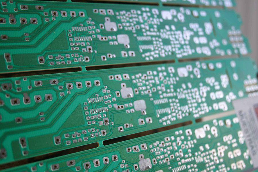
PCB composition and some main functions
The PCB composition consists of main pads, vias, mounting holes, wires, components, connectors, fills, and electrical boundaries. The main functions of each component are as follows:
- Pad: A metal hole used to solder the component leads.
- Via: A metal hole used to connect the component leads between layers.
- Mounting holes: for fixing printed circuit boards.
- Wire: An electrical network copper film used to connect component leads.
- Connector: A component used to connect between boards.
- Filling: Copper for the grounding network can effectively reduce the impedance.
- Electrical Boundary: Used to determine the size of the board, and all components on the board must not exceed this boundary.
PCB composition structure includes Single Layer PCB, Double Layer PCB, and Multi-Layer PCB, a brief description of the three layers as follows:
- (1) Single-layer board: a circuit board in which only one side is coated with copper and the other side is not coated with copper. Usually, the components are placed on the side without copper, and the copper side is mainly used for wiring and soldering.
- (2) Double-layer board: that is, a circuit board with copper on both sides usually referred to as a top layer and a bottom layer (Bottom Layer). Generally, the top layer is used as a component surface, and the bottom layer is used as a component soldering surface.
- (3) Multi-layer board: a circuit board containing a plurality of working layers, which includes a plurality of intermediate layers in addition to the top layer and the bottom layer, and the intermediate layer can be used as a wiring layer, a signal layer, a power layer, a ground layer, and the like. The layers are insulated from each other and the layer to layer connection is typically achieved by vias.
The PCB composition consists of many types of working layers, such as a signal layer, protective layer, silkscreen layer, internal layer, etc. The functions of various levels are briefly introduced as follows:
- (1) Signal layer: mainly used to place components or wiring. Protel DXP usually contains 30 middle layers, namely Mid Layer1~Mid Layer30. The middle layer is used to arrange signal lines, and the top and bottom layers are used to place components or copper.
- (2) Protective layer: It is mainly used to ensure that the tin plate on the circuit board is not tinned, thus ensuring the reliability of the circuit board operation. Top Paste and Bottom Pastes are top solder mask and bottom solder mask respectively; Top Solder and Bottom Solder are solder paste protective layer and underlying solder paste protective layer.
- (3) Silkscreen layer: It is mainly used to print the serial number, production number, company name, etc. of components on the printed circuit board.
- (4) Internal layer: mainly used as a signal wiring layer, Protel DXP contains a total of 16 internal layers.
- (5) Other layers: mainly includes 4 types of layers.
Drill Guide: Mainly used for drilling holes on printed circuit boards.


