Issues to be considered during the design of printed circuit boards
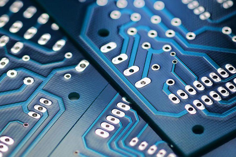
Printed circuit boards (PCBs) are by far the most common method of assembling modern electronic circuits. Comprised of a sandwich of one or more insulating layers and one or more copper layers that contain the signal traces and the powers and grounds, the design of the layout of printed circuit boards can be as demanding as the design of the electrical circuit.
- Make sure that the circuit schematic component graphic is consistent with the real object and the correctness of the network connection in the circuit schematic.
- the design of the printed circuit board is not only to consider the network connection relationship of the schematic diagram but also to consider some requirements of the circuit engineering, the requirements of the circuit engineering are mainly the width of the power line, the ground line, and some other wires, the connection of the line, High-frequency characteristics of some components, impedance of components, anti-jamming, etc.
- the requirements of the printed circuit board system installation, mainly consider the installation hole, plug, positioning hole, reference point, etc. must meet the requirements, the placement of various components and accurately installed in the specified position, while at the same time Installation, system commissioning, and ventilation.
- the manufacturability of the printed circuit board and its technical requirements, to be familiar with the design specifications and meet the production process requirements, so that the designed printed circuit board can be smoothly produced.
- in the consideration of components in the production, it is easy to install, debug, repair, and at the same time printed circuit board graphics, pads, vias, etc. to standard, to ensure that components do not collide, and easy to install.
- The purpose of designing a printed circuit board is mainly application, so we should consider its practicability and reliability, while reducing the board layer and area of the printed circuit board, thereby reducing the cost, the appropriate larger pad, Through holes and traces, are beneficial to improve reliability, reduce vias, optimize routing, make it dense and uniform, and have good consistency so that the overall layout of the board is beautiful. In order to achieve the intended purpose of the designed circuit board, the overall layout of the printed circuit board and the placement of components play a key role, which directly affects the installation, reliability, ventilation and heat dissipation of the entire printed circuit boards. rate.


