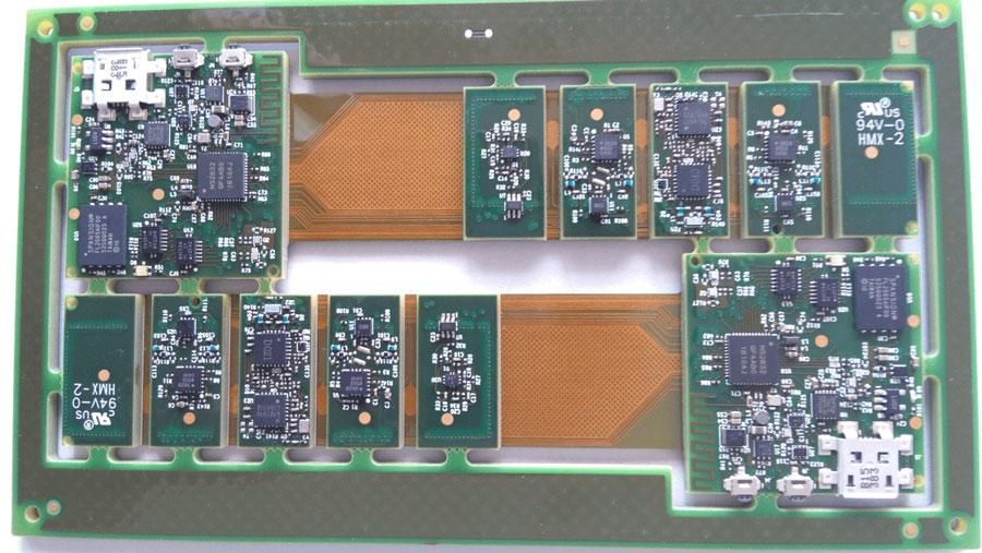
A Guide to Cross-Hatched Planes in Your Flex PCB
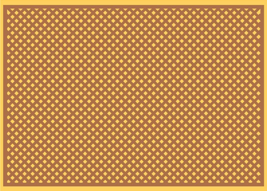
Cross-hatched planes in flex PCB consist of latticework of copper on the surface. Flex PCB with cross-hatched planes involves openings at regular intervals. The use of cross-hatched planes is common in flex and rigid-flex circuit boards.
The hatch pattern offers dual benefits to flex PCB. The special latticework provides ground benefits and also offers structural support. In this blog post, you will learn about the construction, benefits, and design of cross-hatched planes in flex PCB.
Construction of Cross-Hatched Planes in Flex PCB
Cross-hatched planes involve a latticework of copper on top of a flex PCB with openings at regular spacings. The process of designing a cross-hatched design for flex PCB occurs in the CAM or CAD design. The region with the cross-hatched plane is filled with evenly spaced lines. The crosshatch design is formed by edging the area with a thin border connecting the end of the lines.
The multiplayer flex PCB manufacturing process involves roughening the surface to allow copper to adhere to the resin during lamination. The resulting process results in a smooth copper surface that can undergo the develop, etch, and strip (DES) process.
A drawback with flex PCB is that delamination would occur if the surface wasn’t roughened. The delamination occurred between the copper planes and the laminate of the circuit board. It also resulted in loose adhesion of the component mounting pads on the outer layer causing the pads to become loose during the soldering process.
The adhesion problem also occurs during the manufacturing of the flex PCB laminate. The resins employed by the manufacturer in creating the flex PCB laminate impregnated the glass cloth that is combined with a copper foil piece bonded on each side.
Cross-hatching helps address the adhesion problem with flex PCB. The cross-hatching of the PCB involves small openings on the plan that allow resins to bond to the laminate. The manufacturing process of crosshatch flex PCB does not force the resin to bond with the copper. The particular manufacturing process of crosshatch PCB allows sufficient and strong bond that is distributed throughout the flex PCB that prevents delamination of the bonds.
Another method that addresses the problem of adhesion is the black oxide treatment. Moreover, brown oxide is an alternate treatment to increase the adhesion of copper with the surface. The approaches involve micro-etching the copper allowing it to bond with the resin. The methods that allow a strong adhesion between the surface and the teeth of the resin are carried out just before the lamination but after the etching process.
The rough nature of copper can be a problem with high-speed signal devices. This issue is resolved by tracing the surface with a special application of a bond film.
Application of Cross-Hatched Planes in Flex PCB
Modern cross-hatched flex PCB involves an application of the crosshatch on the planes of the inner layers. The outer layer is filled with copper fills. The manufacturing process is applied for both rigid-flex and flex PCB.
A hatch ground method involves a controlled impedance in the flex regions. A reference place is created that is required for a controlled impedance in high-speed flex PCB. The method helps in retaining the flexibility of the assembly and allowing manufacturable dimensions for the flex PCB and assembly.
The cross-hatching process results in a reduced amount of copper required for the board. This results in increased impedance but reduces the capacitance of the board.
The application of the crosshatch design results in improved structural support for the flex areas. The Crosshatch method provides a static or dynamic flex ribbon without increasing the copper layer rigidity on a two-sided circuit.
The layer of the flex PCB can help in the routing of controlled impedance. The correct impedance is important to avoid excessive rigidity that could damage the ribbon. Manufacturers use a modeling tool to identify missing copper in the cross-hatched design.
As the impedance of a trace on a hatched ground is greater than the solid region on the ground, the inductance of the flex PCB trace is decreased for maintaining the required level of impedance. So, manufacturers make the trace lane wider to decrease the inductance and also increase the net capacitance concerning the hatched ground. The method contributes to the required value of the impedance of the crosshatched flex PCB.
Characteristics of Crosshatched Planes in Flex PCB
One of the common characteristics of crosshatched design is a mesh of copper layers in a perpendicular position. Each conductor is placed at about 45 degrees angle. Some of the crosshatched flex PCB have circular openings while others have diamond shapes.
Most crosshatched flex PCBs have a square opening. But the function of the patterns is the same. The design is better for flex PCB as compared to the solid plane design. Solid planes may be more efficient for rigid PCBs but they are too rigid for flex PCBs. Crosshatched patterns result in improved performance, particularly impedance as compared to solid planes.
The copper content of hatched planes is low resulting in lower costs for flex PCBs. The design of the circuit board also provides more flexibility to the designers during the fabrication process of flex PCB. A manufacturer may implement a hybrid approach that involves using cross-hatched design for areas that require bending and a solid plane for region sections of the printed board. The result is the optimum return path and shielding for the circuit board.
Achieving Maximum Impedance with Crosshatched Plane Flex PCB Design
The main reason designers go for cross-hatched planes in flex PCB is to manage the impedance. The design allows a return path for signals that result in maximum impedance. With cross-hatched flex PCB there is no need to increase the dielectric thickness, select a lower dielectric constant or reduce signal line width.
Dielectric constants of flex PCB are small, but the laminate is thin. Designers can not get more than a 0.005-inch distance from the plane to the signals with the flex PCB design. The line width can be reduced for mechanical purposes but this will adversely affect the flexibility of the board in bending.
Crosshatch flex PCB design can help in keeping the traces wide without losing the impedance.
Let’s suppose that a differential pair has a space of 0.006 inches that has a half-ounce of copper on a 0.03 inches substance. The impedance will be 88 ohms for a solid plan microstrip. The impedance increases to 100 ohms when a crosshatch design is implemented with 0.06 inches line and 0.020 inches pitch.
The impedance will be 72 ohms for a solid plane strip line pair of 0.006 inches lines and the same size space between them with a 0.03 inches substrate on a half-ounce copper. The impedance will increase to 82 ohms with a crosshatched pattern of 0.020 inches pitch and 0.006 inches lines. By adjusting the signal line width to 0.0045 inches and the space to 0.009 inches, the impedance increases to 100 ohms.
Another way to achieve maximum impedance with cross hatch flex PCB is to let the line size and space at 0.006 inches and the hatch pattern to 0.040 inches pitch.
Challenges with Crosshatch Flex PCB Design
One of the drawbacks of crosshatch flex PCB design is that it does not provide similar EMI shielding as a solid plane. The design does reduce the wavelength. This depends on the operating frequencies of the operating environment.
Yet another drawback with the hatched flex PCB design is that the signal losses are greater than the solid plane designs. The weak signal is due to the pattern design that alters the return path. Although the loss is manageable, it should be accounted for when designing a flex PCB.
Flex PCB allows the use of wilder traces. The result is a loss in the conductor related to the flex PCB. But they also provide greater flexibility due to thinner dielectrics. The tradeoff negates the negative point of crosshatched flex PCB design.
When designing crosshatched pattern flex PCB, the route pairs on the patterns should be symmetrical to avoid skewness. The return path will be different for the conductor than for the partner if a conductor in a pair is offset from the pattern of the hatch design flex PCB.
The hatch design pattern may be present in the flex portion of the flex PCB or the pattern may extend throughout the rigid section. The pattern is generally extended to the rigid section of the flex PCB to achieve the target impedance values after selecting a particular material.
Generally, cross-hatched pattern design results in good results with improved flexibility. When the impedance is necessary, the flex design can be important for meeting the desired impedance values while remaining flexible for installation.
Crosshatched pattern for flex PCB provides a functional method of controlling the impedance traces. The method allows optimum impedance to be achieved without increasing the width of the traces. The major tradeoff of the crosshatched patterns is that the goal of achieving flexibility is achieved while maintaining acceptable performance.
The line widths of the flex PCB design are kept reasonable with reasonable geometrics on the interposer boards.
Rules With Crosshatch Design Flex PCB
Certain rules must be followed with the flex PCB design board. The rules should be abided by to ensure that optimum performance is achieved. The priority with flex PCB design includes solid planes, cosplayers, and crosshatch. The cosplayers can be with or without the lower ground and are recommended for low layer count for the flex PCB.
The Crosshatch return path is difficult to design and model. But the above method will help in achieving the desired performance levels while retaining flexibility characteristics. Users can lay out the crosshatch pattern and traces as per the recommended hatch configuration.
An important point to remember when designing the cross-hatch pattern for flex PCB is to use it with a combination of solid planes design. The hybrid design will help in retaining the best return paths while achieving flexibility in the required areas.
Crosshatch design should be considered as an alternative to the coplanar structures. The impact of the crosshatch takes effect by managing the field solver engine. Moreover, the crosshatch pattern should be no more or less than 45 degrees for optimal performance.
Another recommendation is that trace alignment should be maintained. The trace alignment should be over the intersections of the crosshatch flex PCB. The traces should also be balanced for differential pairs through a symmetrical intersection of the trace element.
The symmetry of the Return Path with Flex PCB
The symmetry of the return path and trace width is critical for the differential pair. Controlling the return path with a flex PCB requires careful evaluation of the design elements. Trace separation must be considered to make sure that the traces of the pair cross the hatch while maintaining symmetry. Following the recommendation is important to ensure that the traces remain balanced.
Assembly software used to design crosshatch flex PCB will display warnings in case of unbalanced traces. The warning signs can guide the designers to ensure symmetry when designing the crosshatch patterned flex PCB.
The design software allows the specification of a hatch with copper coverage. It is recommended that the copper coverage for the hatch should not be less than 40 percent. The crosshatch of the flex PCB with low copper coverage will not result in the best return path.
The layer-to-layer registration between the crosshatch and the trace is critical during the design of flex PCB. The fabricator capabilities will design the specific registration between the trace and the pattern.
The impedance control issue exists if the design is too stiff for the flex PCB. Overcoming the problem requires selective bonding and debonding of portions of the flex PCB area. The approach will have a better impact than going for a crosshatch pattern for the entirety of the flex PCB. The designer of the flex PCB must take care that the unbonded area doesn’t buckle thereby creating additional space between the substrates. It is important to select the substrate level carefully to ensure that the target return path and signal efficiencies are achieved.
The designer must assess the substrates that should be unbonded for ensuring the optimum return path and signal strength. Hatch ground planes must have proper adhesion of resins to ensure that the copper foils attach to the flex PCB. This consideration is important when designing multilayer flex PCB circuits.
Proper adhesion of the copper is important during the delamination of the internal layers. The layers need to be properly bonded to ensure that the copper sticks to the resin for a secure bond. The crosshatch planes in the multilayer circuit board are necessary with the crosshatch flex PCB design.
During the design phase, manufacturers need to make sure that the polyimide region of the flex PCB remains flexible. The space between the layers that are created when the circuit buckles will prevent symmetry. The symmetry can be maintained by selecting bonding that ensures flexibility without affecting performance.
The planes used for the return path can be used for noise control with crosshatch flex PCB design. The flex PCB is suitable when the signals of the return oath are low.
The approach of crosshatch design is also suitable for multiple plane layers. Using the correct method will have a significant impact on the flexibility of the circuit. It affects whether the flex PCB can be flexed and bent.
The area of the circuit that does not undergo compressing forces tends to experience a shift from the neutral bending axis with a solid plane. The reason is that solid planes have greater resistance than flex PCB. A noticeable shift in the neutral axis can result in stress on the weak conductors, particularly on the outside of the bends.
With crosshatched planes in flex PCB, the copper is removed during the design resulting in the formation of a trace layer with optimum impedance levels. The axis shift of the flex PCB plane is reduced which allows the circuit to be more tolerant and flexible to bend.
The screened conductive epoxy of a crosshatched plane in flex PCB can serve as the shield layer. The method will result in a slight increase in cost. But it will allow increased flexibility of the flex PCB design.
Achieving Flexibility of Flex PCB in Crosshatch Design
The flexibility gained during the crosshatch design process depends on the percentage of copper that is excluded from the flex PCB layer. As an example, suppose that the flex PCB has four layers but there is only one plane. There will be little flexibility by removing 30 percent of the copper from the plane layer. At the same time, if several places have to be crosshatched, a noticeable improvement in flexibility will be achieved with the removal of 70 percent of copper.
Various other concerns should also be addressed when designing the cross-hatch flex PCB. The impedance control of the crosshatched plane of flex PCB will have a significant impact on the impedance value.
Remember that the impedance of the crosshatched flex PCB is directly impacted by the capacitance. More precisely, the capacitance formed between the return path and the transmission line affects the impedance of the flex PCB. The impedance of flex PCB will increase with the decrease in the capacitance of the board.
The capacitance of the flex PCB depends on the area as well as the distance between the two conductors. As a result, decreasing the copper in the return path in cross-hatched planes of flex PCB will result in reduced capacitance.
The characteristic impedance of a crosshatched flex PCB will increase with the decrease in copper from the path. But this does not mean that the impedance can be increased without making the circuit thicker. The reason is that different factors affect the impedance in a cross-hatched place of flex PCB.
The basic assumption is of a solid fill on the layer of the plane. The reason for the assumption is that the circuit of flex PCB generally uses crosshatched planes to make the circuit flexible. The rigid PCB does not require this flexibility due to which a solid shield is used.
The flex PCB industry is in great demand. But the market is not great enough to invest in R&D for finding the optimal value for variable cross-hatched design. Designers have to determine the optimal value through trial and error. The path of the transmission line of flex PCB can vary widely and depends on the orientation and the pattern.
With flex PCB, the two conductors that are side by side may have different impedance levels. The determining factor is the extent that the plane copper can be paired. As a result, it is difficult to include different possible variations for the crosshatched planes in flex PCB.
The patch between the holes in flex PCB with crosshatch design is different. While the right trace path runs adjacent to the left trace, the discontinuities along the way make it difficult to determine the best path. The holes in the plane and the trace orientation make it challenging to know the ideal impedance level.
Modeling of Crosshatched Planes in Flex PCB
The use of field solvers removed the need for closed-form equations for determining optimum impedance levels for flex PCB. The closed-form equations used in the crosshatch flex PCB fabrication have certain limitations. The limitations in the design of the flex PCB are present with small geometrics. Additionally, flexed PCB design often involves etching taper on the fine line traces.
Today closed form equations are not used when designing crosshatched planes in flex PCB. The design of a flex PCB circuit with closed equations creates difficulties in handling ground planes. The shortcoming in the design of flex PCB with crosshatch design can be overcome using the 2-D field solvers.
Modern Flex PCB fabrication devices use efficient equations that allow crosshatch design with optimum impedance levels. Manufacturers should consider the flex PCB material tolerance when designing the board.
Material tolerance is generally higher with the design of both rigid and flex PCB. The design of the flex PCB requires that manufacturers make consideration of flexibility with high-speed transmission lines. The transmission lines of flex PCB should accommodate the impedance requirements for efficient operations. The variations in the flex PCB substrates are also an important consideration when designing the board. These should be considered at the early stage of the design of flex PCB to address the variations.
An alternate approach for crosshatch flex PCB modeling is to use the XFE technique from Polar instruments. The technique involves using 2-D solvers with multiple passes and a unique algorithm when designing the crosshatch pattern in the flex PCB.
A multi-pass approach is also recommended during the design of crosshatch planes in flex PCB. The technique involves multiple passes with a unique algorithm for correcting deviances over a range of impedance in a controlled environment. The multi-pass approach to flex PCB design results in greater impedance control. It also helps account for greater geometric variances during flex PCB design.
The multi-pass method results in the improved capability to solve obstacles in crosshatch design to achieve flexibility in designing places of flex PCB. The fabricators must compare the measurement data with the cross-section performance of flex PCB. Proper and detailed analysis is important during the design of flex PCB.
Crosshatching for flex PCB requires careful consideration of the pitch and width. Moreover, the geometrics in the design of the flex PCB should also be considered.
Conclusion
Hatched plane flex PCB design results in increased impedance. The design of the flex PCB depends on the hatch opening. The operating frequency and the circuit sensitivity of the flex PCB also determine the efficiency of the cross-hatched design.
The crosshatched design may create some signal problems with flex PCB. But the issue is not significant when the best practices are followed during the design of the flex PCB. The shielding effect of the flex PCB is reduced with the patterned design only if the frequency requirement is high. But with most applications of flex PCB the cross-hatched design does not pose a significant problem.
Flex PCB manufacturers have long demanded a practical and efficient method of controlling impedance. Crosshatch design allows for controlling the impedance without a significant impact on the performance. The method for fabricating flex PCB allows efficient prediction of the impedance of the strip line. Moreover, the crosshatch pattern in flex PCB also allows improved tracing of PCB through the deployment of crosshatched return paths.
The return paths of the crosshatch design are more efficient resulting in increased impedance control when designing the flex PCB. The impedance control is greater with flex PCB design as compared to rigid PCBs. The design may create some challenges but the obstacles can be overcome for the efficient design of flex PCB.
Designers can predict the optimal return path with the crosshatch flex PCB design. They can implement an efficient return path that meets the requirements of flex PCB fabricators. The crosshatched flex PCB design is both efficient and effective in approach.
With the crosshatch flex PCB design, the impedance can be kept at a controllable level. Moreover, crosshatched planes in flex PCB also allow retention of flexibility during the assembly process. The method is popular in circuits with a signal strength of about 2 GHz. The crosshatch flex PCB design results in improved signal integrity with minimum line losses.
Hemeixin PCB provides a range of flex PCB solutions that satisfy requirements for quality boards. We have partnered with leading multinational companies in offering them the best quality rigid and flex PCB. Our high-value end-to-end products meet the requirements of flex PCB with simple and cross-hatched patterns.
Visit the Hemeixin PCB website today to get more information about rigid, flex PCB, blind vias PCB and other solutions.


