Microvia PCB Process Guidelines
High density interconnect PCBs were first innovated in the 1980s when researchers investigated ways of reducing the size of vias. The first HDI PCB was commercially available in 1984 with the Hewlett-Packard laser-drilled FINASTRATE boards, followed by Surface laminar Circuits by IBM YASU in Japan, and the DYCOstrate in Switzerland.
Although mechanical drilling can be used for microvia manufacture, the process is outdated and can leave materials in the hole and result in defects. Instead, designers are recommended to use drilling and copper filing for microvia manufacture.
Laser Drilling
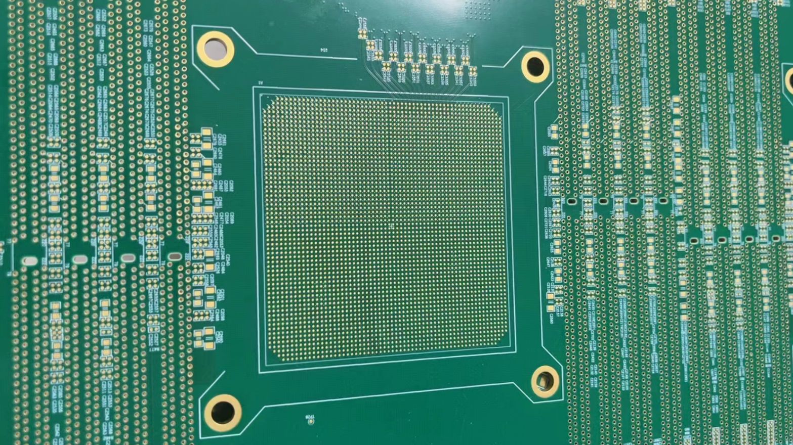
High-density interconnect (HDI) boards require connection holes that have a minimum diameter of 50 μm. Microvias can be drilled in various materials such as FR4, FR5, RCC, Teflon, and Thermount.
When UV laser is used for drilling, the epoxy resin, as well as copper layer and fiberglass substrates, are pierced in a single operation. The energy of the laser should be precisely controlled to minimize damage to the material. The opening of surface copper can be done with the help of wet chemistry or a laser.
The efficiency of laser ablation through the resin can be verified per match using a 3D microscope, SEM, or micro sectioning. The drilling should create a straight hole wall to avoid creating a ‘barrel’ shape and maximize the contact area to the target land. Fabricators may drill the hole at a slight incline (a maximum of 20 degrees) to generate a more conical shape. This can improve chemistry circulation despite the lower contact area.
Low-quality drilling can leave a second glass weave that results in a pronounced conical hole that significantly reduces the contact area to the target pad and an irregular shape of the barrel that does not allow chemistry flow at the later stages of processing.
Another laser process should be applied to clean the target pad (usually UV clean step or a CO2 cleaning step). UV clean step can result in a slight laser ablation of the copper. Fabricators should limit the laser’s energy to enable cleaning the target pad otherwise they could damage the copper of the target land.
The wavelength of the laser’s energy should be in the ultraviolet and infrared region. Laser drilling requires the configuration of the beam fluence's energy and size. High fluence beams can be used to cut through materials such as glass and metal, whereas glow fluence beams can be used to remove organics without damaging metals. A beam spot as small as 1 mil can be used for high energy beams and about 4 mils to 14 mils can be used for low energy beams.
Pro tip: When applying lasers to the PCB, fabricators should not use overhang on the external pad because it cannot be cleaned at later stages of processing. Copper overhang restricts chemistry circulation. Fabricators may utilize copper etching to remove a minute quantity of overhang but it won’t remove all of it. Pre-etching can be used to clear recast copper and resinous debris.
Chemical Desmear
Chemical cleaning or desmear serves as the main cleaning step in the process. Desmear and plasma can be used together depending on the laminate material and the facility’s plasma capacity. A major advantage of using chemical desmear is that it can be used for through holes and can be run both vertically and horizontally. Most horizontal lines will run the despair twice, flipping the board between runs.
Chemical desmearing includes a solvent swell, a neutralizer, and sodium permanganate. Sodium permanganate is used because of its high solubility that prevents flash drying within the microvia during its transfer.
Types of Laser Processes
The two main laser processes use either UV or CO2 technology because they are commercially and economically viable. CO2 lasers can produce microvias in epoxy laminates, however, the copper should be removed from the area that is to be ablated. The CO2 is mostly used for laminates that are incompatible with glass. This includes laminates such as resin coated copper (RCC) foil and flexible polyimide.
Lasers like TEA CO2 (transversely excited atmospheric) use beams at wavelengths of 9000 nm and higher peak power to laze through glass materials.
It is worth noting that there are several variations of lasers but the most popular ones are:
- UV/Excimer
- UV/Yag laser
- CO2 laser
- Yag/CO2
- CO2/TCO2
Ultra violet UV (and other higher power lasers) can be used to remove copper and glass and therefore be used with most laminates, but they are usually very slow when drilling through glass and copper fibers. There are many factors to consider when choosing laser via processing such as:
- Uneven diameter of holes
- Position accuracy of microvia holes (lased holes)
- Dimensional changes to the panel because of variations to the humidity and temperature
- Dimensional changes to the panel after curing
- Unstable nature of negative artwork
- And others
Microetching of Microvias
An important step is the metallization of microvias. The four most popular methods of metallizing interconnect via formation in HDI processes are as follows:
- Electrolysis and electroplating copper
- Conductive graphite
- Electroless Copper (discussed below)
- Conductive Pastes
Electroless Copper
Electroless copper is an alternative process to metallization. The process should be efficient to deposit EC on all of the microvias in a single pass. A double pass may be used to improve inefficiencies such as non-uniform deposition or poor adhesion.
Most experts agree that EC deposition is vital to microvia reliability. The desmear process mentioned earlier is followed by electroless copper deposition. Most desmear copper lines run together with the panels going wet to wet.
The Pros and Cons of Laser Drilling Techniques
All drilling techniques have advantages and disadvantages. The major advantage of lasers is the speed at which microvias can be drilled. The disadvantage is that the copper surface has to be opened with an additional process that can increase time spent in assembly. For best results, it is recommended to use a combination of CO2 laser and UV laser for flexibility and drilling speed.
This allows the microvias to be created in a single working step. Furthermore, the opening of the copper surface is also very precise.
For more information on micro via PCB process guidelines, get in touch with the experts at Hemeixin HDI PCB here.


