What is High-Speed Digital?
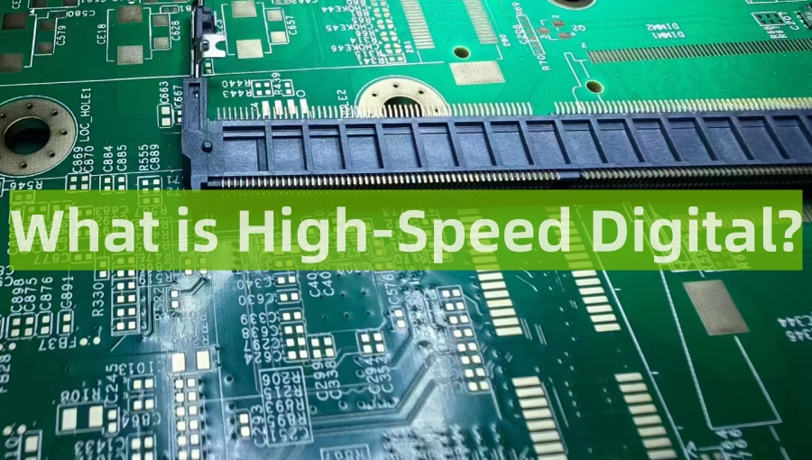
Today, the standards for high-speed digital are evolving much faster than ever, especially to be able to keep up with emerging technologies like the Internet of Things (IoT) and 5G. So what exactly are high-speed digital PCBs? Let's find out!
What is High-Speed Digital?
In our modern world today, we can witness the increasing complexity of electronic products due to the increasing demand for higher performance, including better image transfer, faster data and higher computing power. Most printed circuit boards or PCBs present in these electronic devices are considered to be at risk of at least some type of signal integrity problem. That is what is associated with high-speed digital design - as it itself is focused on creating a circuit board design that is less susceptible to these issues.
As discussed above and quite obvious from the name, high-speed digital is basically a design that corresponds with the systems that use high-speed printed circuit boards (PCBs) and digital signals to transfer data between components. Considering the problems regarding signal integrity in other PCBs, the design, layout and overall concept of high-speed digital PCB basically focuses on creating a circuit board, which is less susceptible to power integrity, signal integrity and EMI/EMC problems.
However, truth be told, no one perfect design is completely free of these problems. But by using the design guidelines for high-speed digital, they can be significantly reduced - in fact, they often become unnoticeable, causing no performance problems in the final product.
The digital world is transforming exponentially, and hence, to make sure our electronic devices are meeting the requirements of technologically advanced solutions, we need the right PCB in them. And that is why high-speed digital and even high-frequency PCB design have become quite a hot topic in the market.
A high-speed digital PCB is basically a printed circuit board that has a digital circuit speed of about 45 to 50 MHZ, and the digital circuit signals take up more than one-third of the entire system.
But it's important to note that there is no one authoritative definition for high-speed digital PCB. Basically, your definition of a high-speed PCB depends on your practice. This started back in the 1960s when digital electronics were still in developmental stages, and signal speed was overall low - hence, PCBs didn't require much effort.
However, later as the digital circuit signal speed elevated, engineers realized traditional PCB designs wouldn't work. Hence, they optimized the circuit design, made use of specific PCB base materials, and developed high-speed circuits - now known as high-speed digital PCB.
The terms "high-speed" digital PCB and high-frequency PCB are often used interchangeably, but the two are quite different. While the two are the same printed circuit boards, they have different meanings. We all know PCBs are circuit boards, and the sine waves are the carrier of the modulated signals. When we say "high speed" digital PCB, we mean the voltage rises and drops in a short period of time.
However, when we say high-frequency, we mean the cycle of the circuit is short. You can say that frequency Is basically the reciprocal of the period here. But the process works something like this: when the frequency of the signals rises, the cycle shortens, which helps ensure there is enough time for the signal to maintain stability, and the time needed for the signals to drop rise also needs to be short. Hence, this leads to high-speed, which shows that a high-frequency PCB is also technically a high-speed digital PCB, and there is no exact distinction between the two.
A Practical Guide to High-Speed Digital PCB Design
Now that you know what a high-speed digital PCB is, it's time to understand its design and see how it works. We know a high-speed digital design system is one that uses high-speed signals to transfer data among components but the distinction between a high-speed digital design and a general circuit board possessing all digital protocols is quite blurry.
Hence, it's important to note that the fundamental metric that denotes any particular system as "high speed" is its rise time (also known as edge rate) of the digital signals in the signal. Other than that, some elements that help determine a high-speed digital PCB are:
- The digital signal frequency is at least 50 MHZ or more
- The time of signal propagation over the track is 1/3 or more, of the signal rise time
- The design uses Ethernet, HDMI, USB, PCI EXPRESS, SATA, Thunderbolt and other such high-speed interfaces that can help transfer data faster
- The size of the PCB is very small
- The circuit consists of various sub-circuits that are each connected to one another through the high-speed interfaces mentioned above
All in all, it can be understood that the high-speed digital PCB design is applied to devices that have a PCB working at high frequency using high-speed interfaces. However, in our era today, most high-speed circuit boards use an RF front end for networking and wireless communication.
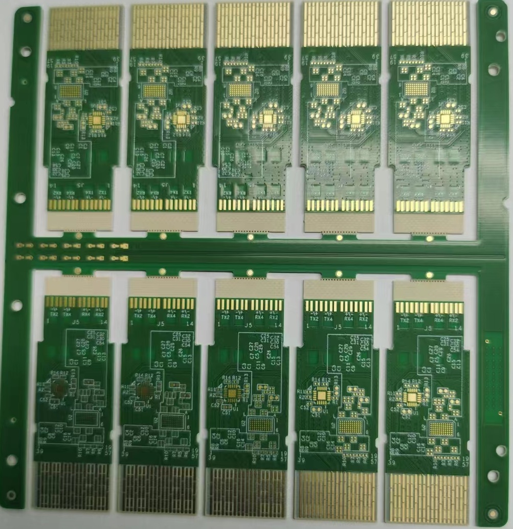
We know that all PCB designs start to form the schematic - a high-speed digital PCB design's major focus is the PCB stack up design, interconnect design and routing. If you are successful in the first two: PCB stack up design and interconnect design, then the third component will be an easy success for you.
When we talk about the design for a high-speed digital PCB, when can go into a lot of depth, but to understand the basics of the design, here are some important steps you must know - that can give you a gist of how a high-speed digital PCB is designed and works.
- Schematic
A good layout and design start with a good schematic. When drawing a schematic, you will need to be focused on the signal flow through the circle - don't forget a schematic with a steady flow will have a good flow on the board as well. Your schematic needs to have all the useful information, including power dissipation, designators, tolerances, etc.
Planning High-Speed Digital PCB Stack up and Impedance
As we said, PCB stack up is an important component, and this is going to be a crucial step, especially in determining impedance and the ease of routing. The stack ups of your PCB will contain several layers - each dedicated to high-speed signals, ground planes and power. Hence, you will need to consider:
- Number of interfaces
- Board size and net count
- Routing density
- Power integrity
- RF signals Low speed
These considerations may need to be modified as per your proposed values because the fabricator will provide the final clearance for the stack up. Once you get the clearance, then you will have to start calculating impedance values.
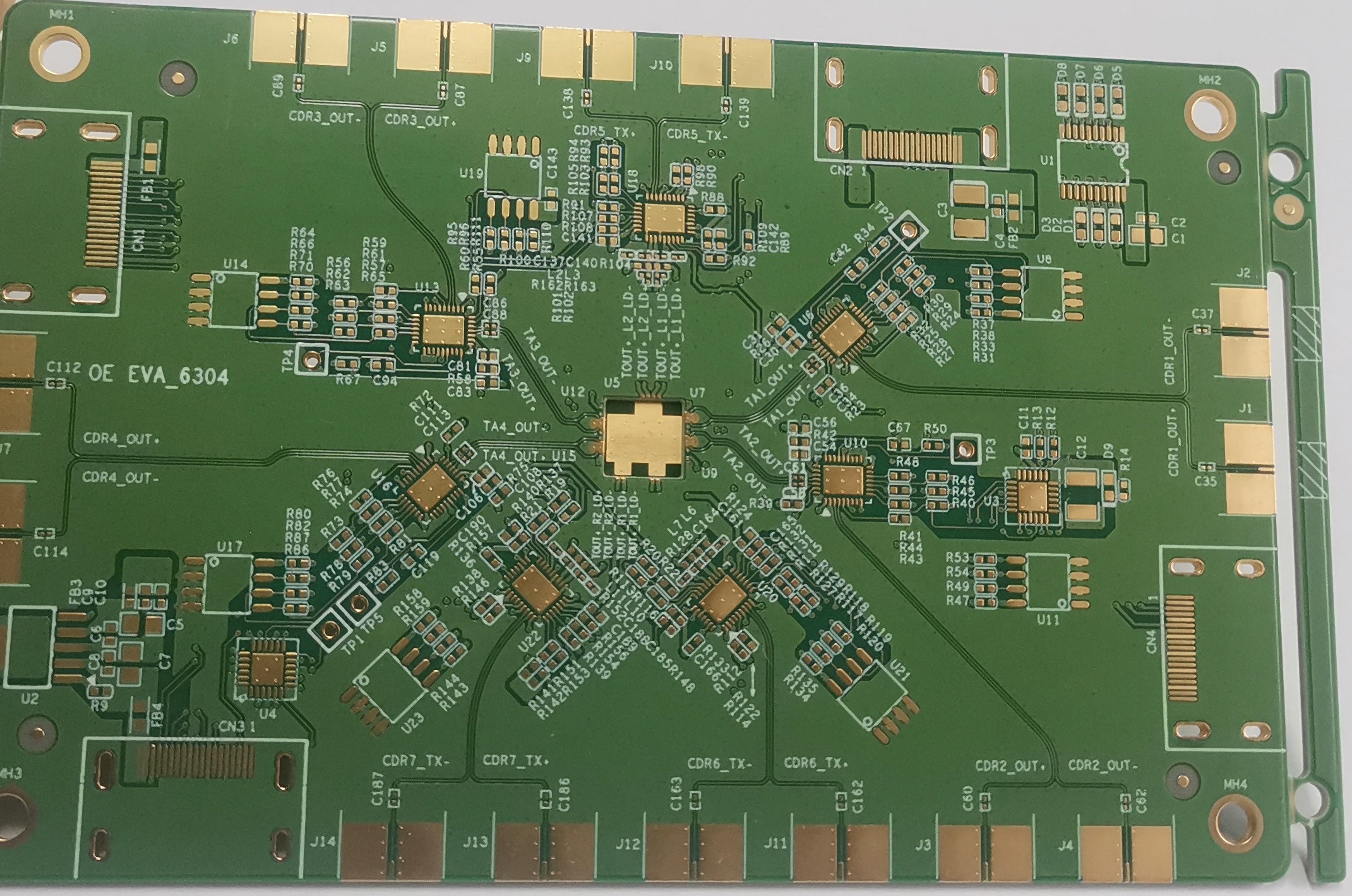
- Floor Planning of the High-Speed Digital PCB
In this step, you will make a floor plan for the placement of the components of the PCB. When it comes to a high-speed digital PCB, do remember there are no specific standards or rules where the components in a high-speed layout should be placed.
However, it's better to place the biggest central processor closest to the centre of the board and the smaller ICs around it. Once all the components are placed, you can set up your high-speed digital PCD design tools that can help you start routing.
- Routine, Power Integrity and Signal Integrity
Signal integrity begins with designing a particular impedance value in the board and maintaining it during routing. Other than that you can also try to minimize the routing through vias, try to aim for shorter routes and eliminate stubs on the ultra-high-speed lines.
For routing, remember the rules you set for designing will make sure you meet your spacing, impedance and length targets while routing your design. Remember, the most important aspect of high-speed digital PCB routing is the placement of ground planes near the traces.
Lastly, ensuring stable power supply and delivery to other high-speed components is critical in the high digital PCB design because power integrity issues often pose signal integrity issues. To make sure you have a stable power supply, use decoupling capacitor groups with a range of self-resonances so that the design will have low impedance.
What is High-Speed Mixed Dielectric PCB?
If you were to break open an electric device today, you will most likely find tiny printed circuit boards (PCBs) in several dimensions inside the device. These PCBs are the building blocks of industrial and consumer electronics - every feature and component of the electronic device maps to the PCB, and one PCB helps provide several features to an electronic system. The point to note here is that the performance and the level of integration of a high-speed digital PCB basically depend on its dielectric material- so what really is a high-speed mixed dielectric PCB?
Well, PCB contains PCB dielectric materials that become the base of the circuit board. The dielectric material is basically a substance, which is a poor conductor of electricity and can be used as an insulating layer for the PCB during the build-up. These materials form a non-conductive substrate layer between the conductive copper layers - making themselves the surface where PCB components are soldered to form the circuit along with the traces connecting each other. Materials like plastics, glass, mica, porcelain and some metal oxides are often used as dielectric materials as they are good insulators and help lower electric loss.
The dielectric constant, also known as the relative permittivity, is basically the electrical property that characterizes the PCB material. The dielectric constant of the dielectric material of the PCB depends on the frequency at which the system is embedded into it.
This constant is known as the measure of the insulation that is provided by the PCB materials. It also shows the degree to which electromagnetic materials slow down the PCB materials because the lower the dielectric loss or energy lost through heat, the higher and more effective the dielectric material. A mixed dielectric PCB is multilayered with multiple laminates and differing dielectric constants.
High-Speed Digital PCB Material
A high-speed digital PCB design consists of multilayers. It entails the use of various materials to create these layers and a layer stack up. In fact, every individual dielectric material has varying material properties. For example, thermal conductivity and dielectric constant.
When designing your PCB for specific applications, make sure to compare the PCB materials and their properties, so you can choose a good material for your circuit base. Other than that, there is various components in a high-speed digital PCB, and you will need to pick the right material for each component to determine temperature rise, interconnect impedance and the roughness of the copper, as well as power and signal loss.
When selecting the materials for your high-speed digital PCB base, you need to consider a lot of factors and material properties to make sure you pick the best that fits into the board's application as per your requirements. Here are some high-speed digital PCB design properties that you must consider:
- Conductor Loss
There are two types of conductor losses. These include DC and AC, and are connected to the conductors’ electrical conductivity and ensure the skin depth. This in turn helps determine the SC losses. Do remember that on the high-speed PCB substrate the conductor loss in copper is related to the copper surface and its roughness. This will increase your system's loss and change your interconnects impedance.
- CTE (Coefficient of Thermal Expansion)
CTE indicates how the printed circuit board (PCB) ) expands as the temperature increases. CTE is antistrophic, meaning the PCB will expand at varying rates and in directions. But, we only need to care about the expansion at the axis which is perpendicular to the surface layer of your high digital PCB alled the z-axis.
Relative Dielectric Constant
This contestant is basically a complex number which consists of the relative permittivity (Dk) and the dissipation factor (Df). The Df value here corresponds to the loss tangent of the material.
- Glass Transition Temperature (Tg)
Glass transition temperature (Tg|) tells you when your Coefficient of Thermal Expansion (CTE) value suddenly increases as the temperature increases. Remember, the CTE value below Tg is smaller than the CTE value above Tg.
Fabricators manufacturing high-speed digital PCB continue discovering better and more suited materials in reference to high-speed circuit boards, high-temperature environments and HDI circuit boards. Besides the base, you also need to make sure you understand the concept of material for stackup. There are standard high-speed digital PCB stackups as industries primarily use FR4 non-conductive materials between the copper layers. But the most major material component of a high-speed digital PCB is polymer resin - as dielectric material - both with and without fillers, metal foil and reinforcements.
Conclusion
High-speed digital PCB is definitely a thing of the future and has great scope for advancement as our technological world keeps advancing. As you can see, when it comes to designing and utilizing a high-speed digital PCB, there are a lot of design considerations and material knowledge that you must know.
Even though we have highlighted the basics of it, there is still much more depth. This is why, if you still have any questions or need help with designing your own high-speed digital PCB, then don't worry and contact us. We will guide you, help you and even design it for you!


