What is Optical PCB?
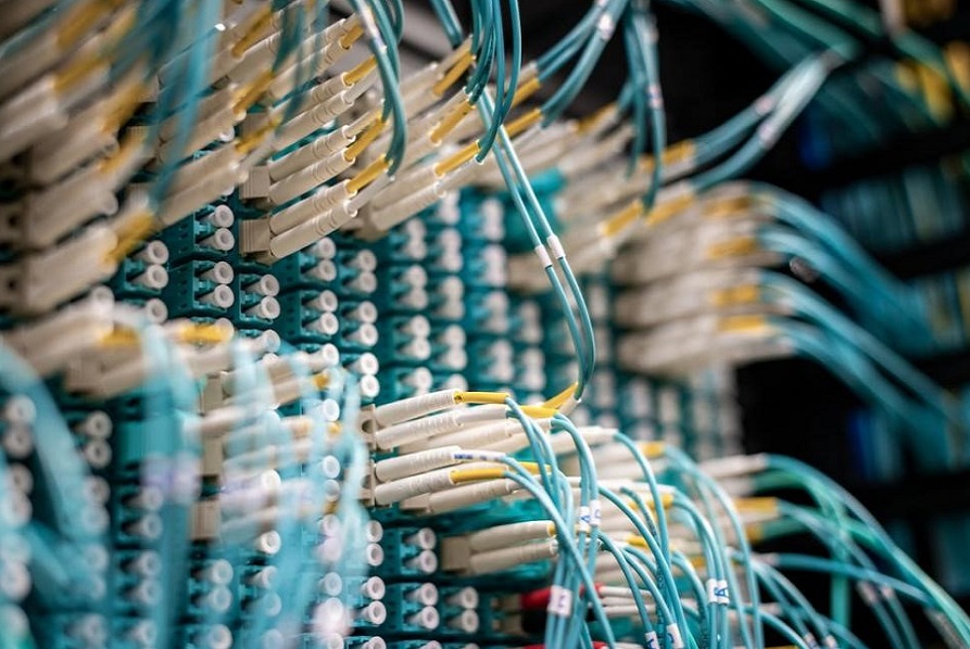
When selecting the right Printed Circuit Board (PCB) for your next project, working knowledge of Optical PCBs is essential. Unlike traditional PCBs that rely on copper traces and electrical components, optical printed circuit boards use fiber optic cabling arranged in a grid-like fashion to interconnect various nodes. With this system, data can be transferred at extremely high speeds without interference or attenuation over long distances - making them the ideal choice for applications requiring fast transmission times.
Optical PCBs, also known as optoelectronics PCBs, are specialized printed circuit boards that transmit and receive light signals. These boards are used in various applications, including telecommunications, medical devices, and military systems.
The history of optical PCBs dates back to the 1960s, when they were first developed to transmit data over long distances using lasers. Optical PCBs have undergone significant technological advancements in the decades since, with new materials and manufacturing techniques developed to improve their performance and reliability.
One major advancement in optical PCB technology has been the development of multi-layer optoelectronic PCBs, which allow for integrating optical and electronic components onto a single board. This has greatly increased the functionality and versatility of these boards, making them suitable for a wider range of applications.
In recent years, there has also been a push towards developing flexible optical PCBs, which have the added advantage of being lightweight and easy to integrate into devices with complex shapes. These boards are made using flexible substrates, such as polyimide or PET, and are ideal for applications where flexibility and durability are required.
Overall, the field of optical PCB has come a long way since its inception, with ongoing research and development leading to the creation of increasingly sophisticated and reliable optoelectronic boards. As technology advances, we will likely see further innovations in this field, opening up new possibilities for using these specialized components in various applications.
Optical PCB Technology

Optical PCB technology refers to designing and manufacturing printed circuit boards (PCBs) that are used to transmit and receive light signals. These boards, also known as optoelectronic PCBs, are used in various applications, including telecommunications, medical devices, and military systems. Optical PCB technology has undergone significant advancements in recent years, with new materials and manufacturing techniques developed to improve these specialized boards' performance and reliability.
Some of the key technological advancements in optical PCB technology include:
1. Multi-Layer Optoelectronic PCBs:
Multi-layer optoelectronic PCBs, or printed circuit boards, are circuit boards that employ light to transmit data or transmit signals. This technology can provide superior signal integrity by using higher speed and potentially greater distances than traditional copper circuits and reducing crosstalk from nearby circuits.
Additionally, due to their thin layers, multi-layer optoelectronic PCBs can be used in physically restricted environments with limited space. The components housed within these boards will benefit from the secure isolation between layers, which keeps the electrical current through it uninterrupted, thus allowing for greater illumination time for each component, resulting in faster transmission speeds and higher overall performance.
2. Flexible Optical PCBs
Flexible optical PCBs are becoming increasingly prevalent in modern electronics and are beginning to revolutionize the sector. These sophisticated devices offer enhanced flexibility and a range of features that traditional PCBs cannot provide.
Flexible optical PCB utilizes specific, transparent materials such as acrylic or clear epoxy fixtures, utilizing cutting-edge photolithography technology and a patented etching technique. This, in turn, allows numerous embedded optical fibers or waveguides necessary for the modulation and transmission of the light signals throughout the circuit pathways.
The increased flexibility makes these boards ideal for use in electronic equipment, which would otherwise be hard to form traditional circuits to fit around without affecting their performance.
3. Photonic Integrated Circuits
Photonic Integrated Circuits (PICs) are compact, cost-effective devices that transmit, route, control, and process optical signals. Their main difference from standard electronic circuits is that PICs utilize light instead of electricity to perform various functions, allowing them to achieve exceptional precision, speed, and stability levels.
Utilizing cutting-edge technologies such as distributed Bragg reflectors, dielectric waveguides, vertical couplers, and electrooptic modulators, PICs enable unprecedented integration densities that allow a wide array of applications from communications to sensing and packaging.
As technology continues to evolve rapidly, we can expect to see more sophisticated photonic integrated circuits making it possible for us and businesses to carry out various tasks faster and with higher efficiency than ever before.
4. High-Speed Optical Interconnects
High-speed optical interconnects are means of communication in which light is used to exchange information between two points faster than with traditional contact-contact electrical connections. They enable data to be sent more rapidly because light can travel considerable distances faster than electricity.
High-speed optical interconnections use lasers, fiber optics, waveguide technology, and polarization components to send data from one interface directly to another without any intermediate conversions or delays. This provides devices with high bandwidth capability and reliability, assuring undistorted signal transmission.
By employing this type of interconnection, it is possible to reduce power consumption, increase system scalability and achieve superior efficiency performance.
Optical PCB Application
Optical PCB has a wide range of applications in various industries, including:
1. Telecommunications
Optical PCB is used in telecommunications systems to transmit data over long distances using lasers or other light-based technologies.
2. Medical Devices
Optical PCB is used in medical devices, such as endoscopes and imaging equipment, to transmit and receive light signals for diagnostic and therapeutic purposes.
3. Military Systems
Optical PCB is used in military systems, such as night vision goggles and radar systems, to transmit and receive light signals for situational awareness and targeting.
4. Consumer Electronics
Optical PCB is used in consumer electronics, such as smartphones and tablets, to transmit and receive data using light-based technologies.
5. Industrial Automation
Optical PCB is used in industrial automation systems to transmit and receive data and control signals using light-based technologies.
6. Automotive
Optical PCB is used in automotive applications, such as head-up displays and advanced driver assistance systems, to transmit and receive light signals for navigation and safety.
Optical PCBs have various applications in various industries, making them an important and versatile technology. As the capabilities and reliability of these boards continue to improve, they will likely be used in an even wider range of applications in the future.
High-Speed PCB Loss Reduction Requirements
High-speed PCB loss reduction refers to minimizing the loss of signal integrity in high-speed printed circuit boards (PCBs). These boards are used in various applications, including telecommunications, computing, and consumer electronics, and are designed to transmit data at high speeds.
The loss of signal integrity can occur due to various factors, including impedance mismatches, crosstalk, and reflections, which can degrade the performance of the PCB and limit its ability to transmit data at high speeds. A number of requirements must be considered to reduce high-speed PCB loss and optimize the performance of these specialized boards.
Some of the key requirements for high-speed PCB loss reduction include the following;
1. Minimal Dielectric Loss
To minimize dielectric losses, high-speed PCBs must be designed with materials that have low dielectric constants and small dissipation factors. The best way to achieve this is to choose materials with high thermal stability and excellent electrical breakdown strength.
For example, Teflon has an exceptionally low dielectric constant (2.1-2.2) and a very low dissipation factor (0.0002). This makes it a great choice for high-speed PCBs.It is also important to ensure that the layers are properly insulated and that there are no gaps between them. This will reduce losses due to radiation and capacitive coupling. Additionally, you should ensure that the materials are compatible with any other components that come into contact with them. This will ensure that the entire system functions optimally.
2. Signal Routing
Controlled impedance is a key component of PCB design regarding high-speed applications. This is because the consistent impedance along the signal path ensures that signals arrive at their destination with minimal distortion.
To achieve this, the line width and thickness of the trace must be carefully calculated to match the desired impedance. This is important for both digital and analog signals, but especially for high-speed digital signals requiring precise timing. To ensure that you meet your desired impedance, use an impedance calculator, which will provide you with exact measurements of the trace width and thickness required. Additionally, ensure that you consider any board stack-up layers or materials that can affect the impedance.
3. Crosstalk Reduction
Crosstalk is the interference of one signal on another due to electromagnetic coupling. It is a major cause of high-speed PCB losses and can be caused by improper PCB layout techniques.
Best way to ensure minimal crosstalk is to use a symmetrical stackup. When designing the layer stackup, pay attention to the directionality of the layers, and try to arrange them as symmetrically as possible. Additionally, pay attention to the spacing between adjacent layers, as this can affect how much crosstalk occurs. When routing traces, it's important to keep them as short and straight as possible, as this reduces the amount of crosstalk by their inductance. Additionally, ensure to route parallel traces at least 5 miles away from each other, and add shielding when necessary. Finally, make sure that components are separated and isolated from each other to prevent interference.
4. Material Selection
Material selection is one of the most important aspects of high-speed PCB loss reduction. Choosing the right materials for your design to achieve optimal performance is essential. When selecting materials, the dielectric constant (Dk) should be considered. This property measures how much the speed of electrical signals changes when passing through the material. Materials with a low Dk are better suited for high-speed designs, as the signals will travel faster through them.
The thickness of the substrate should also be considered. Thinner substrates allow less signal loss due to reduced crosstalk between adjacent traces and lower capacitive coupling. Thicker substrates are better for EMI suppression.
Choosing materials with a high glass transition temperature (Tg) is also important. This ensures that the material remains stable during thermal cycles and prevents the warping of the PCB. The glass transition temperature is also related to thermal expansion, so the choice of material should account for this too.
Finally, the copper foil should be selected with care. Copper has a low resistance, which allows for high-speed signals and low power losses. Choosing the right materials for your design is crucial for achieving optimal performance.
5. Use Ground Planes
When designing a high-speed PCB, it is important to consider the use of ground planes. Ground planes are metal planes that provide a ground reference throughout the board, reducing noise and improving signal integrity. They also help to reduce crosstalk between adjacent signals. They can significantly reduce signal loss in your high-speed PCB when used properly.
To get the most out of ground planes, ensure that the plane is properly connected to all components' power and ground pins. This connection should be as direct as possible, without any vias or other connections. If possible, the plane should also be continuous and uninterrupted to provide the best signal integrity.
To further improve signal integrity, it is recommended to ensure that the power and ground traces are as wide as possible. Ground planes are a great tool for reducing signal loss in a high-speed PCB, but care should be taken when using them. Ensure that your power and ground traces are properly connected to the plane and wide enough to reduce impedance. Lastly, keep all high-frequency components away from the ground plane to reduce interference.
6. Coefficient of Thermal Expansion
The coefficient of thermal expansion (CTE) measures the change in a material's size as it is subjected to changes in temperature. In the context of high-speed printed circuit board (PCB) design, the CTE of the materials used in the PCB is an important consideration for minimizing loss and optimizing performance.
The CTE of a material can affect the performance of a high-speed PCB in several ways. For example, suppose the CTE of the PCB materials does not match the CTE of the components. In that case, the PCB may experience thermal expansion or contraction that can cause stress on the components, leading to reliability issues and potential failure.
In addition, mismatched CTEs can cause shifts in the placement of components, which can affect signal integrity and cause loss.
Optical Interconnects in PCB Design
Optical interconnects in PCB design are an emerging technology that allows the transfer of optical signals through electrical-optic connections using fiber optics or waveguides. They can be used to increase signal speed and reduce electromagnetic interference, making them particularly suitable for high-speed data transmissions 18Gbps and up.
Optical interconnects are often used in place of traditional electrical connectors, such as coaxial cables or twisted pair wires, due to their ability to transmit data at much higher speeds and over longer distances. In addition, optical interconnects offer several benefits over traditional connectors, including high speed, increased durability, and cost-effectiveness.
Why Embedded Optical Interconnects in PCBs for Ultra High-Speed Design
Incorporating embedded optical interconnects into printed circuit boards (PCB) enables ultra-high-speed communications and improved system durability and reliability.
Unlike copper interconnects that tend to degrade over time through electrical noise, embedded optical interconnects remain reliable for years due to their low power consumption and immunity to electromagnetic interference.
Moreover, embedded optical interconnects can transfer large amounts of data at higher speeds than their traditional copper counterparts. This is especially beneficial in applications such as networking, data centers, and servers, which require significant bandwidth or where signals must travel long distances.
Although the cost of design and implementation may be higher initially, the increased latency and performance of embedded optical interconnects will benefit many high-speed designs.
1. Rogers 4350 vs. fr4
Rogers 4350 and FR4 are both materials used to manufacture printed circuit boards (PCBs). Both materials have a range of properties that make them suitable for use in different applications.
Rogers 4350 is a type of high-frequency dielectric material commonly used to manufacture high-speed PCBs. It has a low loss tangent and high thermal stability, making it ideal for use in applications where high-speed transmission and stability are important.
FR4, on the other hand, is a type of fiberglass-reinforced epoxy laminate commonly used to manufacture PCBs. It has a relatively high loss tangent and is not as stable as Rogers 4350, but it is much less expensive and is widely available. FR4 is commonly used in various applications, including consumer electronics, industrial control systems, and automotive electronics.
The choice between Rogers 4350 and FR4 will depend on the application's specific requirements and acceptable trade-offs. Rogers 4350 may be a better choice for high-speed applications that require low loss and high stability, while FR4 may be a more cost-effective option for applications that do not require the same level of performance.
2. Megtron 6 vs.Rogers 4350
Megtron 6 and Rogers 4350 are a dynamic duo for those designing printed circuit boards (PCBs), both materials specifically designed to handle the rigors of high-speed applications. Their unique properties distinguish them; Megatron withstands higher temperatures while Rogers provides optimal signal transmission.
Megtron 6 provides a versatile and reliable solution for the needs of manufacturers of high-speed PCBs. Highly efficient, possessing both low-loss tangent and thermal stability capabilities, Megtron 6 also boasts impressive water absorption resistance and excellent dimensional stability - all ideal qualities sought after when superior performance is required.
Rogers 4350 is renowned for its impressive speed-supporting features. It boasts an impressively low loss tangent, high thermal stability, and good electrical/mechanical properties - making it perfect for applications requiring the utmost performance in reliability and endurance.
The choice between Rogers 4350 and Megtron depends on the application's specific requirements.
3. fr4 dielectric constant at 10 GHz
The dielectric constant of FR4, a type of fiberglass-reinforced epoxy laminate commonly used in PCBs, varies depending on several factors, including the frequency of the signal being transmitted. At a frequency of 10 GHz, the dielectric constant of FR4 is typically around 4.4. This value can vary slightly depending on the specific formulation of the FR4 material and the manufacturing process used.
The dielectric constant of FR4 is generally considered to be relatively high, which can have some implications for the design of PCBs. For example, it can lead to increased losses at high frequencies, which can affect the signal integrity of the board. It can also cause some amount of capacitive coupling between adjacent traces, which can lead to crosstalk.
Overall, the dielectric constant of FR4 at 10 GHz is generally considered to be relatively high, which can impact a PCB's performance. This is one of the factors that must be considered when designing a PCB using FR4 material.
4. fr4 dielectric constant vs. temperature
The dielectric constant of FR4 varies depending on several factors, including temperature. As the temperature of FR4 increases, its dielectric constant tends to decrease. This is because the molecules in the material become more energetic at higher temperatures, which can reduce the material's ability to store electrical charge.
The temperature coefficient of the dielectric constant of FR4 is typically around -0.3% per degree Celsius. This means that for every increase of 1 degree Celsius in temperature, the dielectric constant of FR4 will decrease by approximately 0.3%.
The temperature coefficient of the dielectric constant of FR4 is generally considered relatively small, which means that the impact of temperature on the dielectric constant of FR4 is generally not a significant concern in most applications. However, it is still something that must be considered when designing a PCB using FR4 material, especially in applications where the temperature may vary significantly.
Electro-Optical PCB material
Electro Optical PCB material is a specialty printed circuit board comprised of several layers of glass-reinforced epoxy laminated with thin copper foil. This type of substrate is ideal for high-speed electronic device applications, such as those with high-frequency signal transmission rates and low crosstalk requirements.
It is also ideal for high precision and low signal loss, given its superior capability to tolerate thermal shock and linear expansion coefficient. Coupled with its high durability, it is an increasingly popular material choice in the manufacture of various types of circuitry.
Wrapping Up!
An optical PCB that uses fiber optic cable instead of electrical wiring to transfer information from one part of the board to another. These boards are becoming increasingly popular as they offer several advantages over traditional PCBs, including higher data rates, lower crosstalk levels, and improved electromagnetic interference immunity. If you're looking for a high-performance solution for your next project, an optical PCB may be the way to go.


