What's HDI?

How Do You Use Blind Vias
Blind vias are an attractive solution when space and cost savings are of primary concern. By creating a link between two individual layers without requiring additional board space, this technology provides a valuable way to reduce overall board size. Unlike a traditional through-hole via, blind vias only travel from one side of the printed circuit board and do not terminate on the opposite side.
If your circuit requires internal connections between components on the same layer. In that case, a blind via may be the answer for providing these connections in areas where the components cannot be moved closer together.
To use blind vias in a PCB design, they must be included in the layout of the PCB. This can typically be done using PCB design software, such as Altium Designer or Cadence Allegro. The designer will specify the size and location of the blind vias on the PCB and any other design elements, such as traces and pads.
The fabrication process of these vias has some specific steps, starting with the drilling of an initial hole; the size and shape of this hole must meet the required tolerances. Afterward, copper plating is applied to electrically connect layers before using a chemical etching process to remove any unwanted material resulting from drilling.
Lastly, along with other final treatments, a sufficient amount of torque must be applied for attaching electrical components to the board; this ensures that blind vias will stay firmly connected during transportation and usage. Therefore, meticulous attention is needed to craft blind vias properly, as even small misalignments could drastically reduce performance and electrical integrity.
Fundamental History and Origin of Blind Vias
The use of blind vias has been around since the 1970s when it was used in aerospace and military applications.One of the earliest examples of a PCB with vias is the UNIVAC 1108 mainframe computer, which was developed in the 1960s. The PCBs used in this computer was composed of multiple layers of printed circuits, with vias used to connect the layers and provide routing for the various signals.
The technology was developed to help reduce weight and improve the ability to route signals between two layers within a printed circuit board (PCB). It enabled a much denser population of components than could be managed with through-hole or surface mount technology.
Due to their versatility, blind vias have become widely used in modern electronic design and development.
In addition to their practical use in creating electrical connections between different layers on a PCB, blind vias are also commonly employed by engineers designing complex systems that require multiple ground or power planes without creating too much clutter or wasted space on the board layouts. This type of via can achieve superior signal isolation compared to traditional through-hole vias since they do not penetrate through the board structure; they only go as deep as necessary.
Today's advancements in blind via technology have allowed engineers to create tighter pitch profiles (the distance between two holes) while maintaining reliable performance characteristics. With this increased capability comes higher requirements for process accuracy during manufacturing—a careful balance must be maintained between drill depth accuracy and hole size uniformity.As technology progresses and continues pushing boundaries—especially at ever-shrinking sizes—blind vias will remain essential for engineers looking to bring complex designs from concept into reality without compromising performance or durability standards.
Blind Via Types
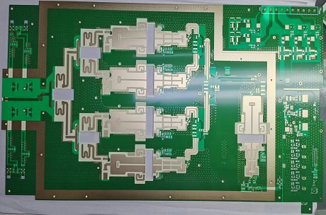
Blind vias, also known as blind microvias, are specialized drill holes used to construct multilayer printed circuit boards. Unlike other types of vias visible on outside layers, blind vias only extend to an interior layer, remaining unseen on the outer portions of the circuit board. These tiny holes enable electrical connection between internal components and external devices or subcomponents, providing additional electrical routing paths for tightly packed printed circuit boards.
Because blind vias can reduce build time and cost, they are commonly used in complex high-density assemblies that require many interconnections. Some of the types include;
1. Sequential Lamination Blind Via
Sequential lamination blind vias are created using a sequential lamination process. This involves bonding multiple PCB layers using heat and pressure and then drilling through the layers to create the via.
Using Sequential Lamination Blind Via technology provides a range of advantages in advanced circuit boards. This advanced process, also known as SLBV, incorporates blind microvias embedded within the panel's core structure to enhance electrical and dimensional performance while saving time and costs associated with production.
Blind vias are drilled without passing through the entire panel, allowing for improved isolation behavior in densely populated PCBs. Moreover, because the drilling and lamination processes are done at intervals rather than simultaneously, it reduces manufacturing complexity compared with another blind via technologies.
By optimizing processes and functions, SLBV helps reduce cycle times by up to 40%, increasing efficiency and providing cost-saving benefits to manufacturers.
2. Controlled Depth Drilled Blind Via
Controlled depth-drilled blind vias are created using a laser or mechanical drilling process. They are called "controlled depth" vias because the depth of the via is carefully controlled during the drilling process to ensure the correct depth for the signals being routed through it.
Controlled depth drilled blind vias are used in high-density interconnect (HDI) PCBs, where space is at a premium, and there is a need to route signals through multiple layers of the PCB. They are often used in conjunction with other via types, such as microvias, to route signals in high-density areas effectively.
One advantage of controlled depth drilled blind vias is that they can be placed closer together than other types of vias, which can be helpful in high-density applications. However, they can be more expensive to manufacture than other types due to the precision required in the drilling process.
3. Laser-Drilled Blind Vias
Laser-drilled blind vias are created using a laser drilling process. A laser is used to precisely drill through the layers of the PCB to create the via.
Laser-Drilled Blind Vias offers designers and manufacturers a compelling advantage relative to traditional through-hole technology. This innovative solution promises the advantages of decreased board sizes and a decrease in trace size, enabling tighter routing and more efficient space allocation. It also boasted higher performance with lower parasitics, improved signal integrity and increased layer utilization when compared to existing through-hole solutions.
Eliminating plating processes further enhances these benefits, allowing PCB assemblies to have shorter lead times with fewer assembly steps than required. These design considerations make Laser-Drilled Blind Vias an ideal choice for many challenging designs.
BGA Breakout and HDI PCB Board Thickness
BGA (ball grid array) is a type of surface mount technology (SMT) packaging used for integrated circuits (ICs). It consists of an array of metal balls on the underside of the IC package that makes contact with the pads on the PCB. To use BGA packages, the PCB must have a corresponding array of pads with a pitch (center-to-center distance between pads) that matches the pitch of the BGA balls.
When designing a PCB with BGA packages, it is important to consider the thickness of the PCB. The PCB must be thick enough to allow the BGA balls to contact the pads but not so thick that it becomes unnecessarily expensive or difficult to manufacture. As a general rule, the PCB thickness should be at least equal to the diameter of the BGA balls plus the depth of the pads.
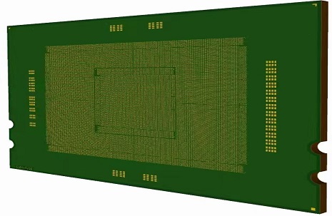
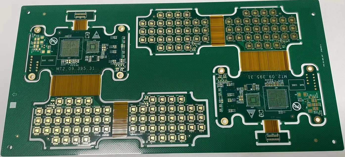
High-density interconnect (HDI) PCBs are specialized printed circuit board form used to facilitate highly complex and intricate designs. Its features allow for a considerable increase in the level of integration of components on the same board. They also make it possible to build circuits where signal transmission is faster and more efficient by providing a direct connection between certain conduction paths with less capacitance, even when dealing with reduced pitches.
The thickness of an HDI PCB will depend on the specific design and manufacturing processes used, as well as the application's performance requirements. HDI PCBs tend to be thinner than traditional PCBs, as they use advanced manufacturing techniques to create smaller, more closely spaced vias and other features. However, the thickness of an HDI PCB will also depend on the number of layers and the overall complexity of the design.
The Electrical Advantages of Blind Vias in Electrical Systems
Blind vias are used in PCB design to connect internal layers of the PCB that are not accessible from the external surface.
There are several benefits to using blind vias in electrical systems:
1. Increased Routing Density
Blind vias allow signals to be routed between internal layers of the PCB, enabling the creation of more complex and densely packed circuit designs. This is particularly useful in high-density applications where many connections are required in a small area.
2. Improved Signal Integrity
By allowing signals to be routed between internal layers, blind vias can improve a circuit's signal integrity by reducing the signal path's length. This can be especially important in high-speed or high-frequency applications.
3. Greater Design Flexibility
Blind vias provide more routing options and greater design flexibility, as they allow connections to be made between layers that are not accessible from the external surface of the PCB.
4. Reduced Size and Weight
By enabling the creation of more densely packed circuit designs, blind vias can help to reduce the size and weight of electrical systems. This is particularly useful in portable or space-constrained applications.
5. Enhanced Reliability
Blind vias can improve the reliability of a circuit by reducing the number of external connections and providing a more robust and secure connection between internal layers.
The Shortcomings of Blind Vias
While blind vias have many benefits, they also have shortcomings that must be considered when deciding whether to use them in a PCB design.
1. Limited Layer Count
The use of blind vias is generally limited to PCBs with a relatively small number of layers (typically up to 8 layers). This is because the manufacturing process becomes increasingly complex and expensive as the number of layers increases.
2. Limited Aspect Ratio
The aspect ratio (hole diameter to board thickness) of a blind via is limited by the manufacturing process. As the aspect ratio increases, it becomes more difficult to fill the via with conductive material and achieve a reliable connection. This limits blind vias in applications where large hole size is required relative to the board thickness.
3. Increased Design Complexity
The use of blind vias can add complexity to the PCB design process, as the designer must carefully consider the placement and size of the vias to ensure that they do not interfere with other elements of the circuit. This can add time and cost to the design process.
4. Reliability Concerns
There is a risk of reliability issues with blind vias, as the manufacturing process involves drilling through the PCB and filling the holes with conductive material. If the via is not properly filled or the connection is not robust, it can result in a failure of the circuit.
5. Process Limitations
The use of blind vias is generally limited to certain PCB fabrication processes. For example, some processes may not accurately reproduce the fine feature sizes and close tolerances required for blind vias.
Blind Vias Gone Bad
Several potential problems can arise when using blind vias in a printed circuit board (PCB) design. Some of the most common issues include:
- Via misalignment.
- Via underfill
- Via overfill
- Via collapse
- Via bridging
- Via wicking
To avoid these problems, it is important to carefully design and manufacture the blind vias, using appropriate materials and processes to ensure a reliable connection. In addition, it is important to thoroughly test the PCB to identify any problems with the vias or other components of the circuit.
Are Blind Vias Expensive?
Blind vias can be more expensive than through-hole vias, requiring additional processing steps and specialized equipment. The cost of a blind via will depend on several factors, including the size and aspect ratio (hole diameter to board thickness) of the via, the number of vias required, and the overall complexity of the PCB design.
In general, the use of blind vias can add to the cost of a PCB, particularly in designs with a large number of vias or in applications where high-precision manufacturing is required. However, the increased routing density and design flexibility that blind vias provide can also offer cost benefits in certain applications, such as by reducing the size and weight of the PCB or by enabling the use of more densely packed components.
IPC Warning About Blind Microvia Reliability for High-Performance Products
The IPC (International Association for the Advancement of Electronic Packaging) is a trade association that sets standards for the electronics industry. In 2017, the IPC published a technical report (IPC-7220) warning about the reliability of blind microvias (small diameter vias that terminate at an internal layer of a PCB) in high-performance products.
According to the report, blind microvias can be prone to reliability issues due to their small size and the high aspect ratio (hole diameter to board thickness.The report recommends that designers take steps to ensure the reliability of blind microvias in high-performance products, such as using a larger via size and aspect ratio, implementing proper design and manufacturing processes, and performing thorough testing and evaluation of the PCBs.
Wrapping Up!
In a world where speed and convenience are king, HDI provides the necessary means to get products to market quickly while maintaining high-reliability standards. When time is of the essence, HDI offers an ideal solution that doesn’t sacrifice quality or performance.


