PCB Assembly and PCB Fabrication
If you prototype printed circuit boards and PCB assembly in China, how can you ensure that laminates and prepregs you used will match those used in offshore volume production?
As an industry, those of us involved in designing and manufacturing electronic products can all agree that we now live and operate in a global supply chain environment. Since a lot of what is incorporated into current and next-generation products is reflected in the software, this isn’t much of a concern. Take your favorite products, download the latest software update and newly developed apps and you’re ready to go.
When it comes to developing the pieces of hardware, the process is not so simple. And, when it comes to printed circuit board (PCB) development efforts, the process becomes even more challenging. That’s because PCBs are the launching points for hardware product development and the laminate and prepreg materials used in designing and manufacturing PCBs are the nuclei for those boards. (Prepreg is fiberglass cloth that has been saturated with resin that is not fully cured. As a PCB is placed under the heat and pressure of lamination this resin melts and flows into the voids in the adjacent copper layers filling them.)
Semiconductor chip technology has become so advanced that testing these highly complex devices must be performed effectively to ensure high reliability and functionality. This allows chipmakers to convey to their OEM customers their highest confidences that their products are of the foremost quality and have been verified to operate according to their specifications.
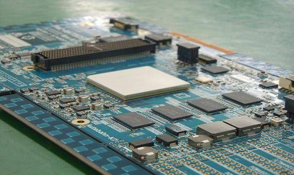
An automatic test equipment printed circuit board, or ATE PCB — serving as an interface to a large test system — is at the heart of all major test activities to verify a specific chip’s functionality.
This assures chipmakers their semiconductor products are good-to-go to an ever- burgeoning chip market led by newcomers, such as Internet of Things (IoT), wearables, handheld devices, and other similar products.
ATE PCBs are designed and assembled to test an array of different semiconductor chips, including microprocessors (µPs), memory, system-on-a-chip (SoC), field-programmable gate arrays (FPGAs), and others. However, an ATE PCB is designed and assembled specifically to test one particular kind of chip set. Some of today’s highly advanced chips bring tens of millions of dollars into a chipmaker’s coffers.
In order to achieve that highly-prized chip-testing quality for chipmakers, a group of experienced program and project managers and highly-trained and savvy engineering personnel in ATE PCB assembly are of paramount importance. The requirements for disciplined administration management and assembly line technical knowhow are above and beyond that required for conventional PCB assembly. Considerable monetary loss and lost time-to-market are incurred if there’s a misstep along the way toward successful assembly completion of an ATE PCB.


