Flex PCB design guidelines
The purpose of this design guide is to enable you to design a highly reliable, flex PCB optimized for manufacturability.
This guide provides technological data for choosing the appropriate materials, and recommendations for their correct design, while taking into account their integration criteria and constraints through assembly processes and car environment.
What is flex circuit
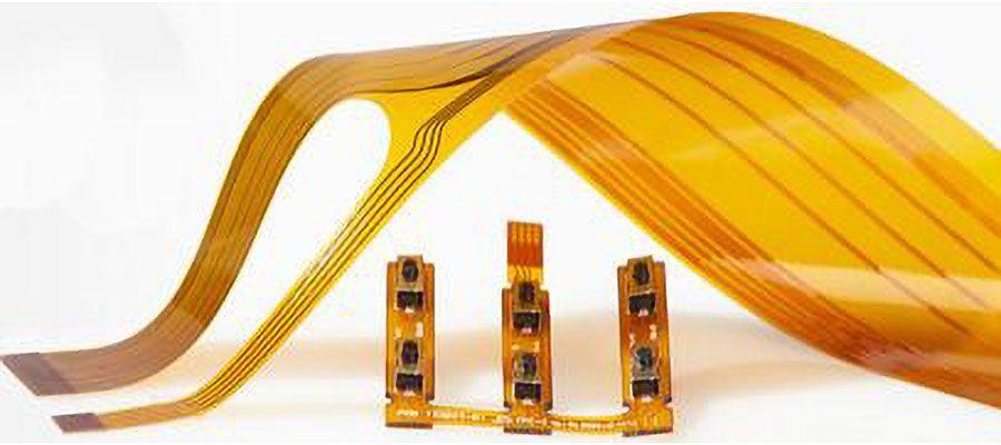
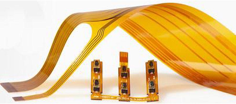
Flexible circuit boards are your go-to-choice when you need PCBs to offer you the freedom of shaping them into different configurations. In fact, Flex PCBs derive their name from their capability to ensure that the circuitry can be designed to fit the electronic device instead of building the device in a manner in which it fits the circuitry. With a malleable base material, flexible printed circuit boards are a popular choice as they offer enhanced capabilities to suit today’s complex and miniature appliances. With the design freedom that they offer, flexible printed circuit boards result in lightweight and durable products. From wearable technology to medical equipment, its use is ubiquitous as it helps retain the precision of a regular PCB while offering unlimited freedom as far as the packaging geometry is concerned.
Flex Circuit Design Advantages
The fact that a flex can be bent, folded and configured in just about any shape or thickness imaginable gives the designer tremendous options when creating an electronics package. Size and space limitations are far less of an issue than traditional design using hardboard circuits. Assembly and handling costs can be significantly decreased because the entire interconnect system can be built as one integrated part. Add hemeixinpcb’s ability for component assembly and testing and the supply chain management becomes greatly simplified.
Below flex circuit guildelines including these contents:
-
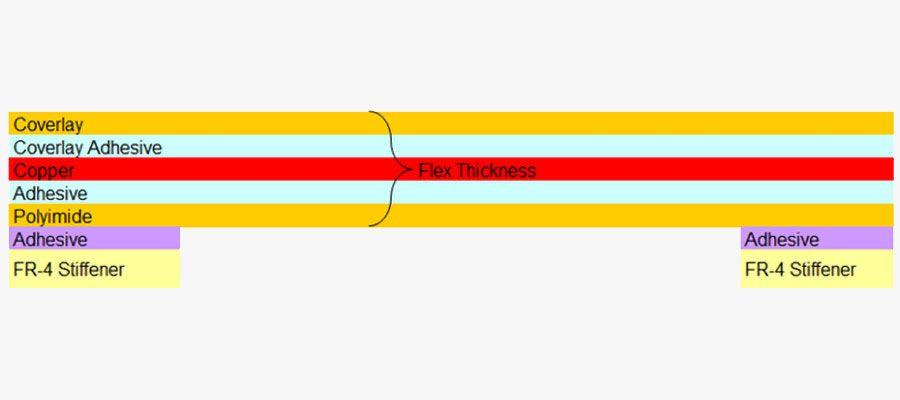
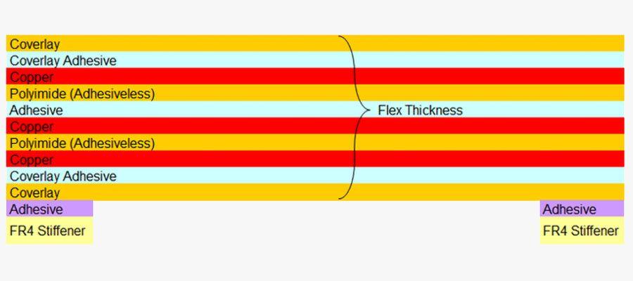
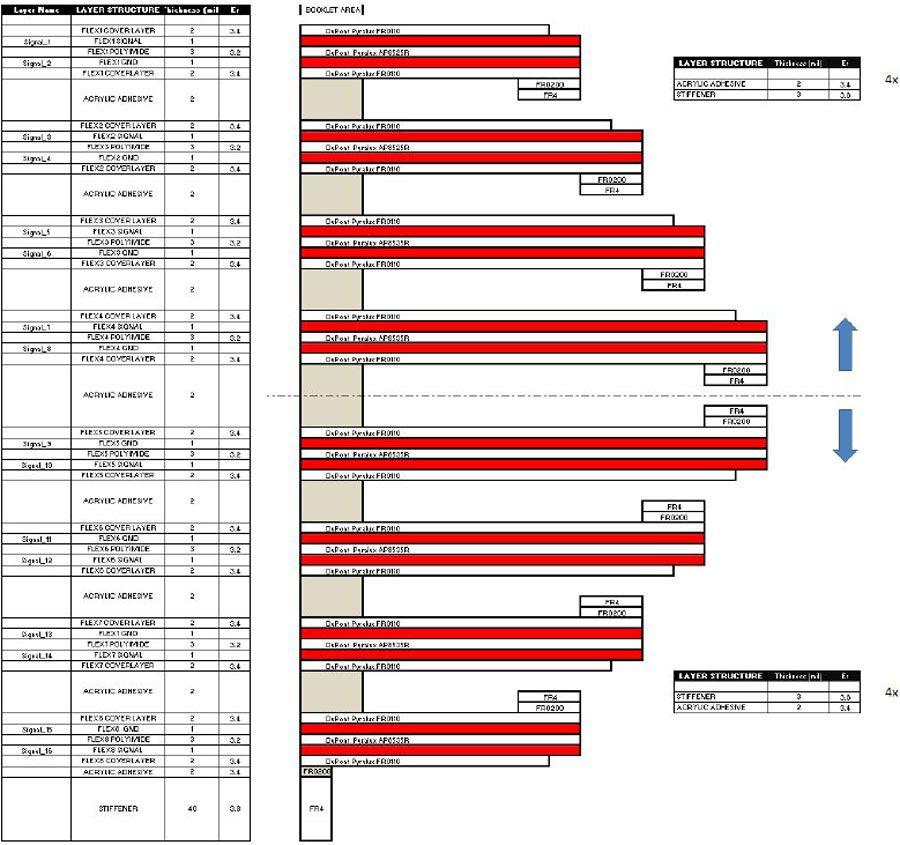
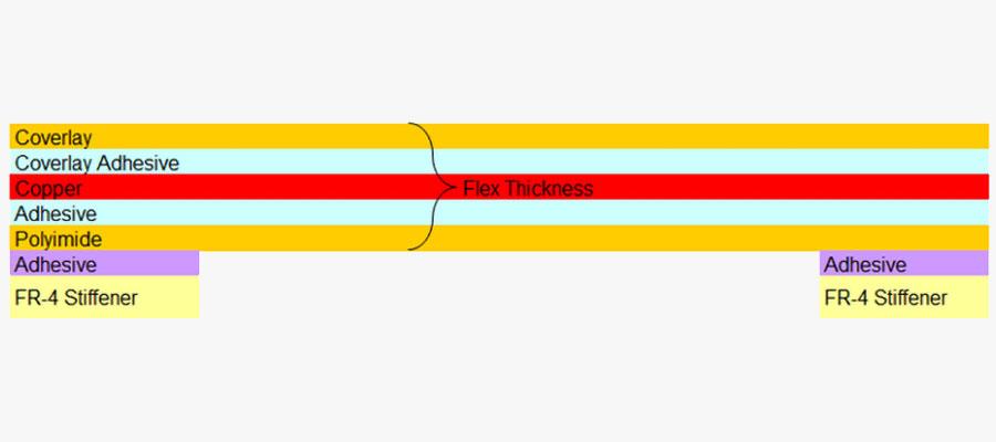
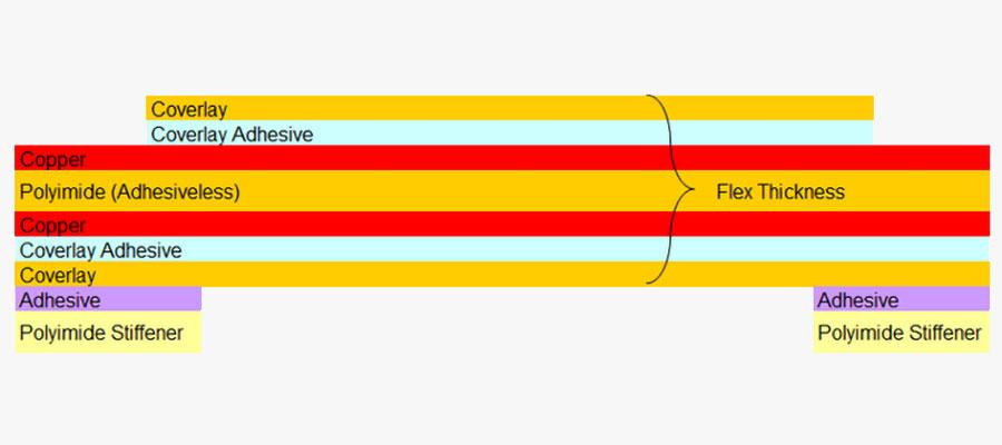
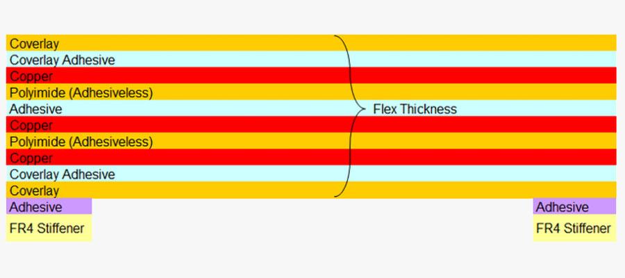
Flex pcb board standard stack up
-
Flexible pcb production process flow
-
Flexible circuit Design Guides and Rules
Flex Circuit Board Types or Flex pcb Construction
There are numerous types of flexible circuits that can be designed according to the needs of the customer. Given below are a few basic types:
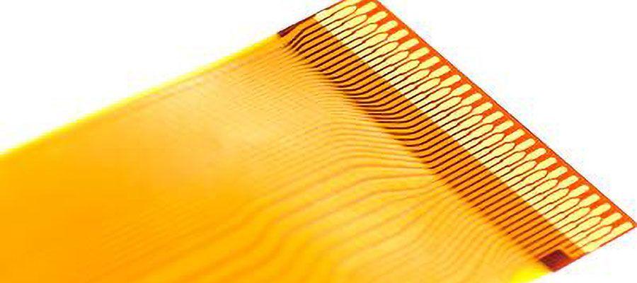
Single Sided Flex: This is a flex circuit that comprises a conductive layer of copper on one side of the PCB. Single sided circuit PCBs are ideal for dynamic applications, or equipment that require circuits with high levels of flexibility. They are known for their immense cost-effectiveness and ease of assembly. Single sided flex PCBs require one type of tooling. Hence, multiple copies of the PCB can be reproduced. They are the ideal solution for replacing wire harnesses.
Double Sided Flex: An expansion on the singled sided flex PCB, the double sided flex comprises a conductive layer of copper on both sides of the PCB. Generally, the copper layers are connected to each other by Plate Through Holes (PTH) or vias. These holes or vias create an active circuitry between the layers. This is one of the most popular flex designs, and is known for its ease of manufacturing. Double sided flex circuits are designed to be light weight, and provide benefits of reproducibility.
Multi-Layer Flex: As the name suggests, multi-layer flex circuits comprise more than two copper conductors. In a typical circuit, you will find up to 10 conductive layers. Like the double sided flex circuit boards, multi-layer PCBs are interconnected by PTH holes or Vias. The multi-layer design is ideal for applications that require PCBs with high density connectors, and the conductors need to be routed through a small area. The PTH mounting method helps create a more reliable solder joint.
Rigid Flex Circuit Boards: This circuit is a combination of rigid and flexible circuits. The flexible layers are integrated with the rigid layers, and the PCB is assembled using PTH technology. The advantage of this type of circuit is that the combination of rigid and flex layers creates small interconnect areas, which reduces the chances of PCB failure in an application.
High Density Interconnects: Also known as HDI, high density interconnects are flex circuit boards, which are designed to provide more technical solutions in terms of design, layout, and construction. Each HDI includes extremely dense flex circuitry with precise features and microvias. These help achieve the manufacturing of small sized yet powerful PCBs with increased functionality. HDIs are known to provide exceptional electrical performance, improved usage of advanced Integrated Circuits (ICs), and greater PCB reliability.
Single Side Flexible PCB
Double sided flex circuit

Multilayer flexible PCB

Blind and buried via flex circuit
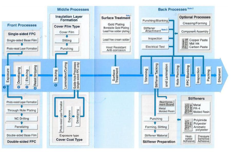
Flex circuit manufacturing process flow

Flex Circuit Design Guides and Rules
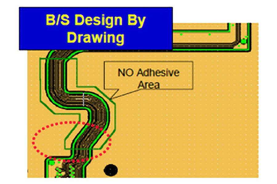
- If the border line type of NO ADHESIVE AREA part is vertical, it can cause SHORT or OPEN circuit problem.
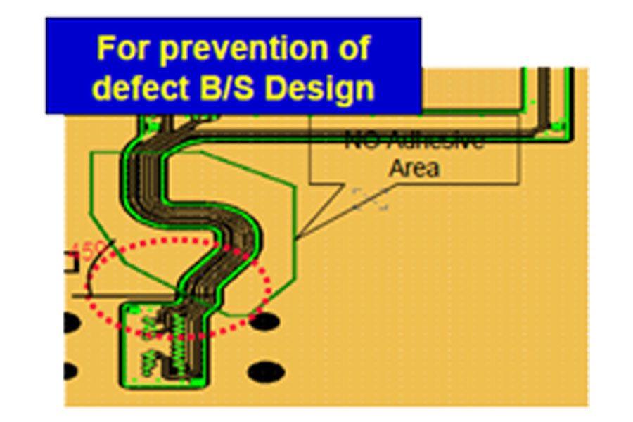
- We prefer to design the Bonding Sheet in the manner that gives a slope of 45 degrees to one of the border lines of LCD mounting area or TAIL part. (Exception: Single sided type may not be affected)
2. Pattern design of Folder Area
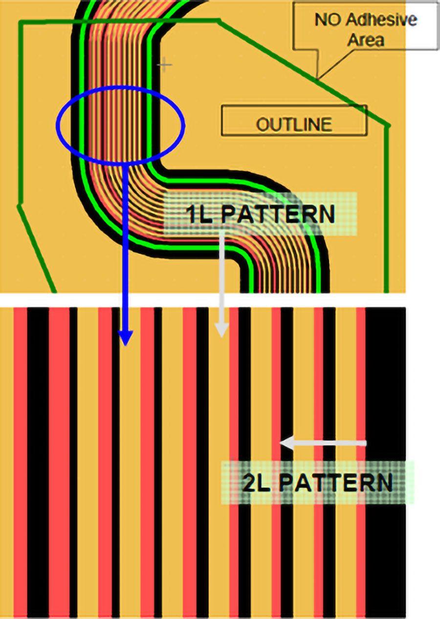
- Purpose: To retain the maximum flexibility by staggering the pattern lines.
- Method:
- Pattern lins on each layer will be staggered. (as much as possible)
- Pattern lines on 1st and 2nd layer are staggered. (Refer to diagram beside)
- Pattern lines on 3rd and 4th layer are staggered. (Refer to diagram beside)
- As result, pattern lines on each layer can be staggered with each other.
- This is to be considered for signal pattern line.
- Reason: If the pattern of every Layer is located above the same line, it causes decreate of flexibility.
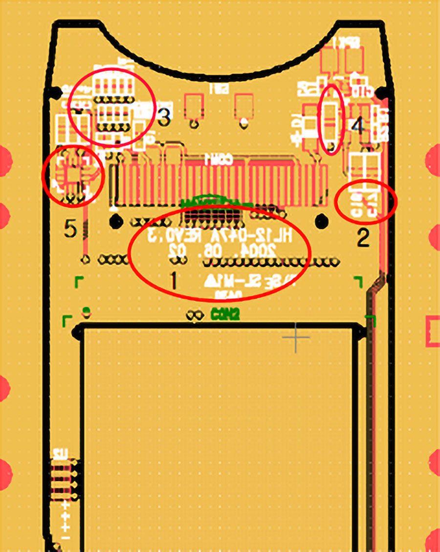
- Purpose: avoid possible default by understanding silk screen production condition.
- Method:
- Text Mark: Customer's mark, Symbol, Date code; Size 2mm
- Component Test Mark: Min. 0.7mm, Max. 1.5mm, We may shift the marking position depending on the situation. (After discussion with the customer)
- Insulation Line:
- Line for preventing short circuit between the lands;
- Line thickness: 0.15mm (standard);
- Distance between line & land: 0.2mm;
- Land Out-Line:
- Silk screening on the outer line of the land is of no use.
- Prefer to remove unless it is an insulation lin (After discussion with the customer).
- Alignment Line: Follow the customer's request.
- Space: Min. 0.2mm between the lines. If it is beyond specification, it will be shifted after approval from customer.
Silk Screen Tolerance
| Item | Dimension |
|---|---|
| A (Min. Width of Marking) | Min. 0.15 mm |
| B (Min. Distance from Land) | Min. 0.2 mm |
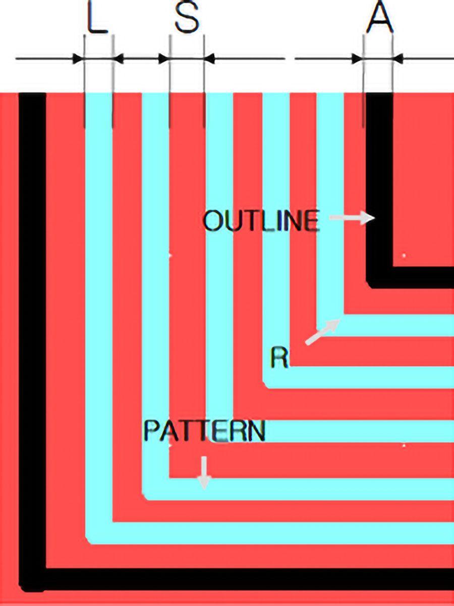
| Two Layer type | L (Min. Line) | S (Space-pattern / Pattern) | A (Space-pattern / Border) | R (Min. Radius Value) |
|---|---|---|---|---|
| 1/2 oz | 0.005 (±10%) | 0.005 | 0.2 | 0.2 |
| 1 oz | 0.075 (±10%) | 0.075 | 0.2 | 0.2 |
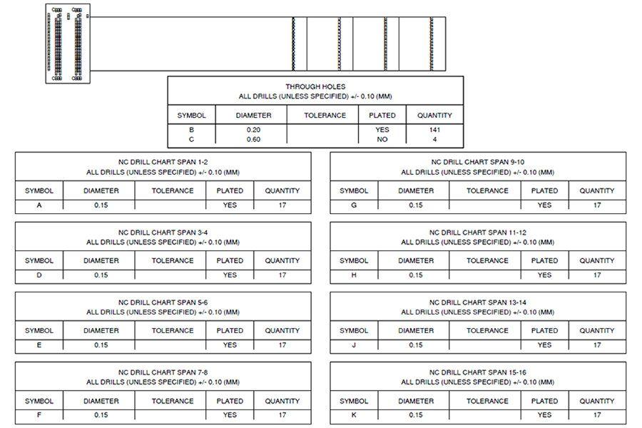
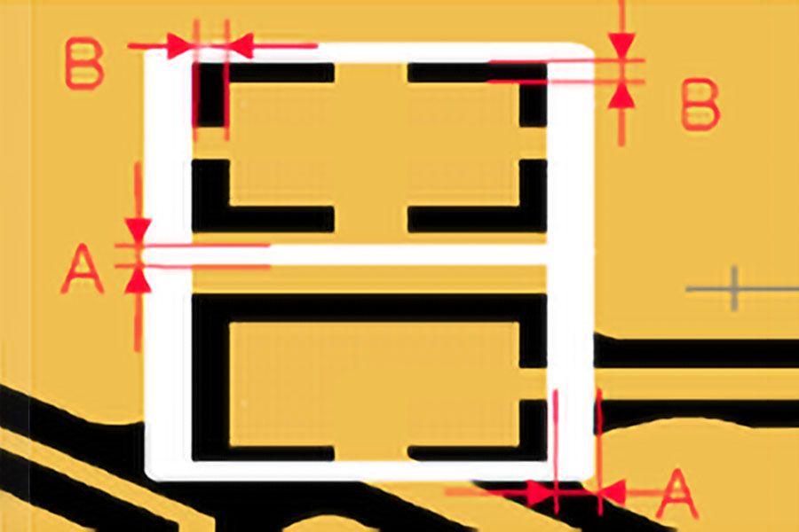
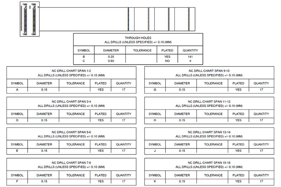
5. Through hole / Pad (Inside)
| Mechanical CNC | Laser N.C | |
|---|---|---|
| A | 0.10 | 0.10 |
| B | 0.40 | 0.30 |
| C | 0.10 | 0.10 |
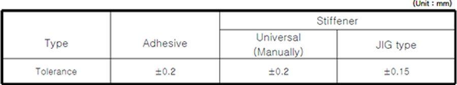
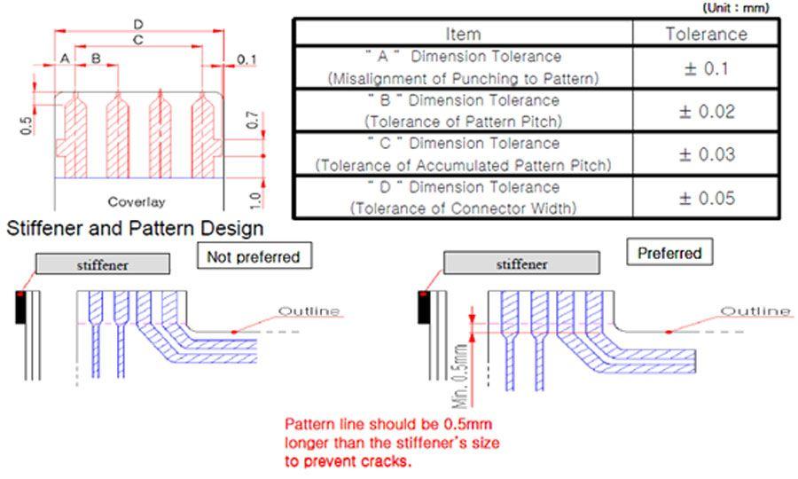
Stiffener / Tape Area Tolerance
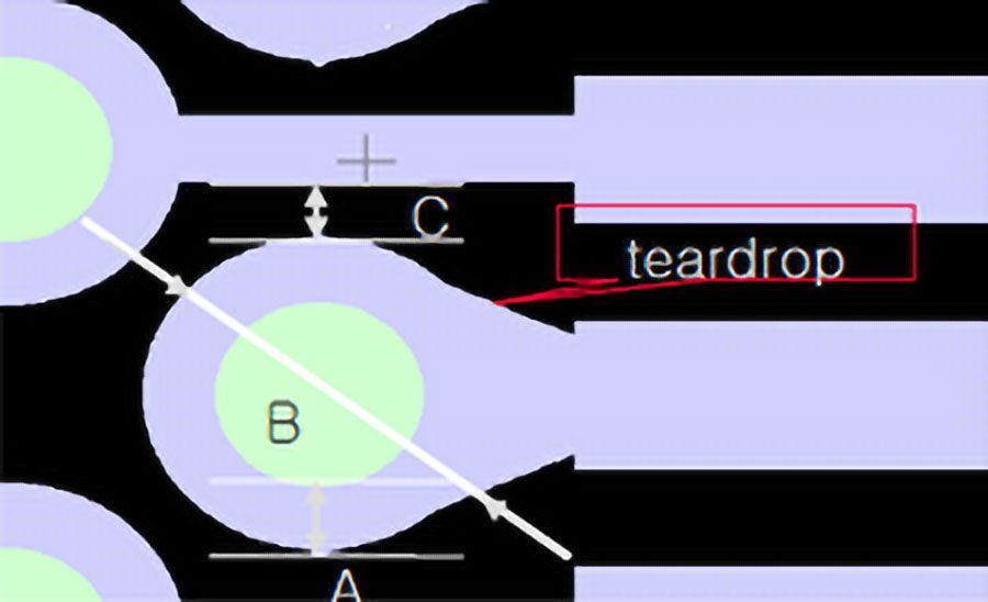
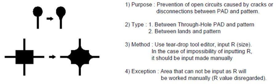
6. Tear-drop design
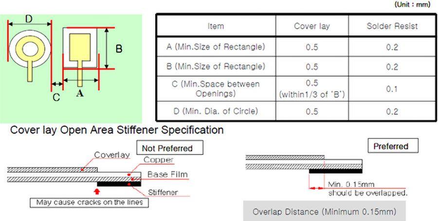
7. Cover lay & Solder Resist Formative Dimension
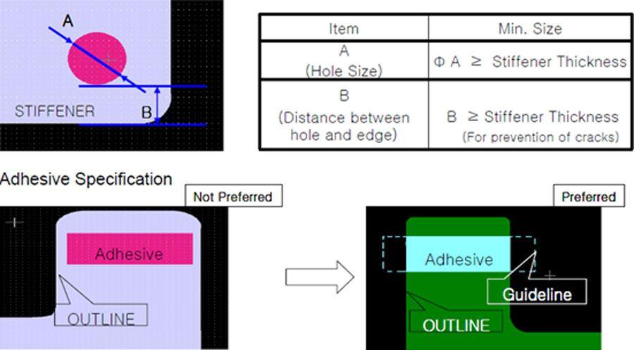
8. Gap from stiffener edge to Hole
9. Gold fingers design
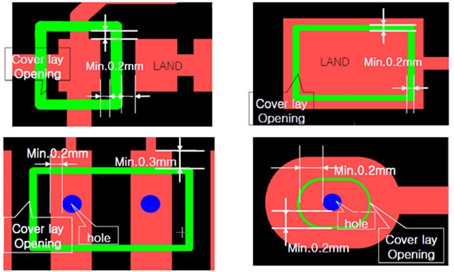
10. Pattern Cover lay Open Area Specification
11. Design in flex pcb bending areas
With as main objective to keep constraints lower than the FPCB copper elongation limit.
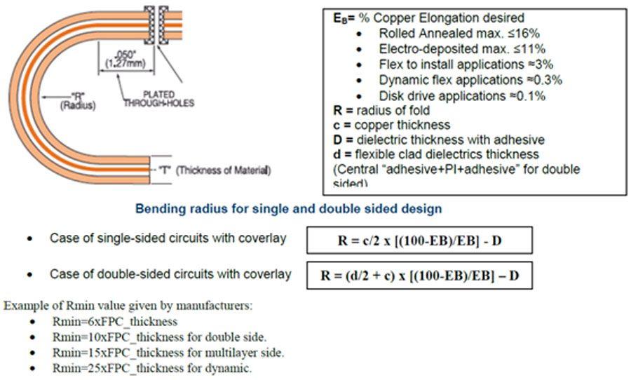
12. Flexible PCB dynamic bending
Depending of the radius fold and cycles number needed the FPCB could be adapted.
For example Hemeixinpcb builds and guarantee FPCB for 100000k cycles into a HDD, and 100k cycles into a mobile phone.
Some data are given for a FPCB double-sided tested with 5mm radius fold:
- PI of 12.5μm, copper of 35μm, coverlay of 12.5μm => 20k cycles
- PI of 25μm, copper of 17.5μm, coverlay of 25μm => 10k cycles
- PI of 12.5μm, copper of 17.5μm, coverlay of 12.5μm => 90k cycles
The most Polyimide thickness used for the base material and for coverlay is 25 μm, but for applications needing more cycle in dynamic bending the use of 12.5 μm must be studied with flex pcb manufacturer. It could rise cycle from 10k to 90k (with copper 17.5μm).
For boards subjected to dynamic bending thinner copper thickness improve the number of cycles. 17.5μm thickness copper is advised and must be studied with manufacturer. Decrease from 35μm to 17.5μm could rise cycle from 20k to 90k (with polyimide 12.5μm)
In this case bend radius calculation (next chapter) must be done with EB=0.3 %
For boards subjected to dynamic bending, tracks on only one side improve number of cycle. If more layer of copper track is needed, staggered tracks are mandatory.
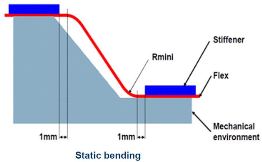
13. Flexible PCB Static bending
For a natural static bending IPC advise not to place components in bending area but manufacturers tested favorably little and not fragile components. They advise to not place them into bending radius lower than 100mm. The placement in concave (inner radius) bending is less restrictive.
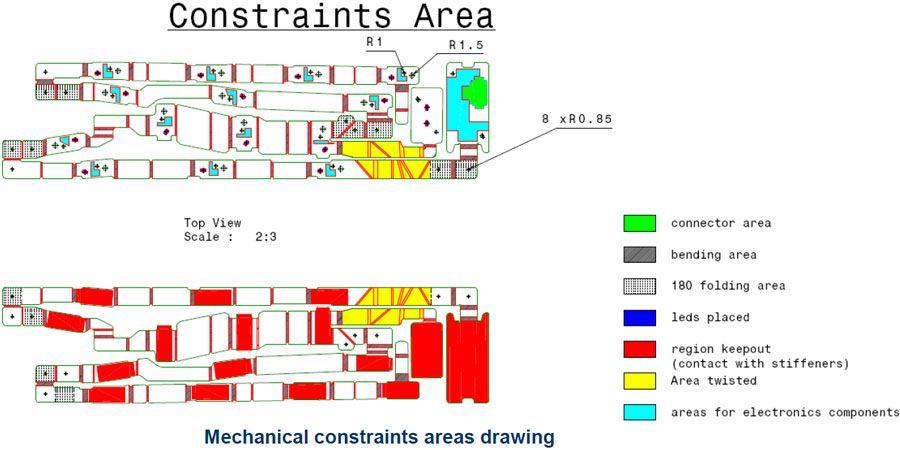
14. Flexible PCB constraints areas
Each area in a flexible circuit has its constraints; the mechanical designer shall give description details depending on the final requirements.
While using this guide, keep in mind that the design information provided is only a suggestion. Hemeixinpcb takes pride in manufacturing flex circuits that are considered difficult to build. In most cases, we do build above and beyond the “standard” circuit specifications, provided that the flex circuit design and type allow for it.
Hemeixin welcomes the opportunity to help you design and manufacture a product that meets or exceeds your expectations. That is why we have established a variety of communication channels to encourage meaningful exchange and dialog. Please send email to This email address is being protected from spambots. You need JavaScript enabled to view it. If you need some supports.


