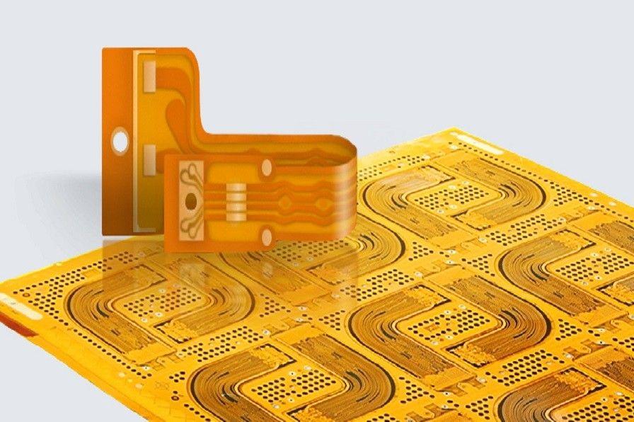
Flex PCB Board FAQ

  • FAQ

What is a flexible circuit?

Also known as flex circuits or flexible electronics; they are thin and lightweight electronic circuits usually constructed with polyimide plastic substrate.

What materials are they made from?

Our flexible circuits are made from a build up of component layers; polyimide, copper, coverlay and stiffeners. These are all bonded together through either an epoxy or acrylic adhesive.
How are they different to rigid PCBs?
Traditional PCBs and Flexible PCBS serve the same purpose so many manufacturing components are the same. Similar tools and technology are used during fabrication and steps relating to the drilling of holes, printing and more apply to both boards. So which type you choose will depend on your application. When the total weight, portability or design space of a device is in consideration, a flexible circuit enables product manufacturers to configure electrical layouts in ways that rigid PCBs cannot.

How much do they weigh?

Flexible circuits weigh less than rigid PCBs yet still offer the same reliability and durability. A lightweight and flexible circuit board can ensure that a smaller product doesn’t increase in weight during manufacturing. A typical flex may be only 100 microns thick whilst the thinnest viable rigid board is around 500 microns.

Are they as strong as rigid PCBs?

In terms of strength under pressure, the flexibility and thinness of the design, flex circuits can cope with the stress of tension, weight pressure and the ability to be bent and curved. Compared to rigid PCBs in this sense it makes them stronger.

Are flexible circuits more expensive than rigid PCBs?

Generally speaking, rigid PCBs cost less than flexible circuits. Be prepared for small runs of flex circuits to be considerably more expensive than a rigid PCB of the same size. Higher volume production run will see prices converging on pricing only a little more than rigid PCBs. However, in terms of costing the whole product you’re creating, it could work out more cost effective to use a flexible PCB rather than having to edit, change and construct new ways of incorporating a rigid PCB. Flexible electronics can reduce the need for a number of components from a design and so the cost of materials and assembly overall can be reduced.

What are the advantages of using flex versus cables?

Flex provides several advantages to cables. We’ve covered the pros and cons of both in our article Flex Circuits Fit Where Cables Cannot. Flex’s higher upfront cost will dramatically reduce cost in the long run. Cables can take several weeks to go through production, while flex PCBs can be completed in several days. In short, using flex eliminates or completely decreases cable cost, reduces assembly time, and produces a lighter end-product.

What are the preferred hole and pad sizes for flexible PCBs?

Some flex materials, like Kapton, do not drill as well as regular materials. 10 mils and above is preferred for minimum size, only in the flex part. Rigid-flex specs are similar to rigid board specs. Pad size, plating process for flex is barrel-only (hole wall).

What are the best flex prepreg materials?

No-flow prepreg is the preferred bonding material for joining flex and rigid materials. This is most commonly found in standard FR-4 or Polyimide.

What are the alternative prepreg materials for joining flex and rigid materials?

No flow prepreg is the preferred bonding material. Available in either standard FR-4 or Polyimide.
What does a real stackup look like? (Not four signal layers, plane layers needed)
The plane layers for the flex are the same as the would be for the rigid board. This board would be turned into a 6 layer board, as follows:

Why aren’t you using coverlay?

Cost, precision, and overall process robustness.
Mask can be used as-submitted, without any additional considerations. This is ideal for customers used to typical pcb processes, and doesn’t require design or library changes to switch to a Flex pcb.
Coverlay requires a number of additional design considerations to avoid manufacturing issues. Since most of our customers do not have design tools that can check for coverlay-specific issues, it would generate a lot of surprising fabrication issues and/or silent changes. We’d prefer to avoid both of these.

What’s the minimum width of a flex strip?

Currently, no official value. Currently, we recommend a minimum of 250mil (6.35mm) to avoid issues with our depanelization and shipping processes.

What’s the minimum bend radius?

This is design and application specific: We recommend reading flex design guidelines before planning any sharp bends, and accounting for each bend individually.
These table should help as a rough guideline to check your calculations. Due to the application specific nature of actual bending, we can make no warranty about correctness.
The bend radius depends on the board thickness of all layers passing through the bend. Multiplying the total thickness by the appropriate “bend ratio” then generates the expected bend radius. See our stackup for details on layer thicknesses. For simplicity, the following calculations include mask on both sides, and the number of copper layers listed.
A “static” bend is intended to be bent into shape and mounted, and is not intended to be bent from that point onward.
Copper Layers in bend Conservative static bend Agressive static bend
1 10:1 ratio, 74mil (1.8796mm) 6:1 ratio, 44mil (1.1176mm)
2 20:1 ratio, 216mil (5.4864mm) 12:1 ratio, 130mil (3.302mm)

A “dynamic” bend will have a bend/straighten cycle during normal operation. Estimating the “dynamic” bend radius is more complicated, and rough guidelines are harder to define. We recommend simply making dynamic bends as large as your application will allow to minimize wear. Sharper dynamic bends will result in decreasing the number of bends a PCB can survive prior to failure.

Copper Layers in bend Agressive dynamic bend
1 10:1 ratio, 74mil (1.8796mm)
2 20:1 ratio, 216mil (5.4864mm)

Note, due to the use of soldermask instead of coverlay, our Flex PCBs are not well suited for use in applications where dynamic bends are used for operationally critical systems, such as medical and industrial.

Are there any design rules for placing parts on the flex circuit?

Place parts where the flex has a stiffener or has been rigidized.

Are there recommended dimensions for the hatch pattern?

8 mils by 8 mils

What is the most cost-effective type of via for HDI rigid-flex designs, stacked microvia or blind/buried vias?

The real cost driver is the number of laminations. Vias should never be in an area that is dynamic. You don’t have to use stiffeners, but we do not suggest it in the flex area. Make sure vias stay out of the bending area as well.

What is the purpose of stiffeners?

First, it is important for you to understand that the PCB stiffener is not an integrated part of the electrical circuit board design. It exists just to offer mechanical support. We call a stiffener for when you need it. Here are some enlisted reasons to call for stiffeners:
  • To strengthen any specific area of the board.
  • To maintain proper thickness in the flex circuit.
  • To support PCB components and connectors.
  • To constrain the flexible parts to areas where they should be.
  • To facilitate better handling of a thin flimsy circuit board.
  • To keep certain areas of flexible circuits flat and stable.
  • To meet ZIF connector specifications.
  • To increase the bend radius of the circuit at the intersection of rigid and flex part. This will avoid the stress on flex part during multiple bending operations.

Basically, you use a stiffener when you require a rigid area in your flex circuit, maybe to protect components or connectors attached there. This will not let the circuit bend and protect the integrity of the part’s solder joint.
Continue reading our guide to PCB stiffeners.

What is the temperature that the rigid flex material usually supports?

Temperature guidelines: Kapton has a high temperature rating but is limited by adhesive.
Copper foil: adhesive or adhesiveless material.
Lead-free: not flame-retardant, has less outgassing (used in the military).

Do S curves in the flex region help with flexibility?

Yes. Making the S curve helps not only with flexibility but also reduces the likelihood of the traces cracking. Placing traces opposite also helps.

Where are dimension tolerances specified?

Rigid-flex can generally can hold the same tolerance as, rigid PCBs. If you are talking about mechanical dimensions, +/- 5 mils is an acceptable tolerance.

How many layers can your flex region have? Can you have hashed ground planes on either side of the signal layers for noise purposes?

The number of layers depends on the design requirements. 12 layers of flex is not unheard of; however, the higher the number of flex layers, the more difficult it is for the PCB to flex. Yes, you can have hashed ground planes on either side of the signal layers.

Is it possible to create a flex section with exposed adhesive so the section can be attached to an interior surface of the enclosure?

Yes, pressure-sensitive adhesive (PSA) can be applied to flex.

How easy is it to attach components?

If this is a feature required, the base material you select must be able to withstand solder temperatures for extra components to be attached. The region in which components are attached are generally “rigidized” because solder joints and components are not flexible, and will fail if they are not mounted on a rigid substrate. Whilst individual flex circuits can be hand assembled, to facilitate machine assembly by SMD pick and place machines, flex circuits must be mounted on or within a rigid carrier panel. Careful design for manufacture will allow simple removal of the finished assemble flex from the mother panel.

How do you add a fully rigid panel around the outside of the rigid-flex design to aid in automated processing?

The rigid part of the board is also part of the array.

What is the difference between assembling flex and rigid boards?

Flex is more difficult to assemble than rigid boards, because it is not as sturdy to assemble. We often create backing or fixtures to add additional reliability before beginning the assembly process.

What is the order of assembly? Are through-holes/vias in the rigid section drilled after the layers are bonded together?

The flex layer is processed first. This makes up one of the layers of the rigid multilayer. Plated through-holes are drilled after lamination.

Do we need tooling holes and fiducials on each rigid section for component assembly?

Fiducials and tooling holes need to be on the rigid section or on the array rails.

Is it best to panelize a flex board, or leave that to the vendor?

Leave it to the vendor. However, the engineer should supply array dimensions.

When manufacturing rigid-flex, how is the rigid part removed around the flex board?

The bonding material (prepreg) is removed from the flex region, and then the rigid part is milled as part of the final route operation.

How to avoid blistering?

Flex material is hydroscopic (it absorbs moisture). Blistering comes from moisture trying to get out, and can cause thermal defects, like substrate blisters and barrel cracking during soldering. It also reduces dielectric breakdown voltage and expands the board. Pre-bake can stop blistering and eliminate moisture absorption.
Copyright © 2024 Hemeixin Electronics Co, Ltd. All Rights Reserved.