Any layer HDI PCB – What it is and how it works
Any Layer HDI, sometimes also called an ELIC – Every Layer Interconnect HDI, is a PCB where each layer is a microvia-based HDI layer, and all the connections between the layers are made using copper filled microvias. This approach has eliminated the need for PTHs for the surface to the bottom layer connection, since both the outer layers can be connected using stacked or staggered copper-filled microvias. This allows for a higher component density by utilizing most of both surfaces.
Any-Layer HDI is still being developed and refined. Fabricators are experimenting with new techniques and materials, like using specialized pastes for interconnects between the layers. But the technology itself isn’t very original. It’s almost two decades old.
The image below shows a side cross-sectional view of an ELIC HDI stackup. This microsection image contains stacked microvias throughout the PCB stackup, but it could also contain staggered microvias in different regions.

Panasonic introduced its first ALIVH (Any Layer Interstitial Via Hole) to the market in 1996.
Any-Layer HDI PCBs have found a special place in smartphones, GPU, and CPU circuits, and it’s easy to see why. If you use Any-Layer HDI method to design and fabricate your PCB, instead of the conventional HDI techniques, you will use about 40% of the PCB volume; this saves precious space for other gadgets in the smartphones, making them lighter overall.
Any-Layer PCBs first mainstream use is usually associated with Apple’s iPhone 4 and iPad 2. Apart from decreasing the volume of the PCB board, the difference in thickness between an ordinary HDI and Any-Layer HDI is also very significant. The iPad 2 was almost 35% (4.6 mm) thinner than the original iPad because iPad 2 employed a 3+4+3 Any-Layer HDI stack up. A relatively latest example is the Samsung Galaxy S8 that uses a 12-layer Any-Layer HDI stack up.
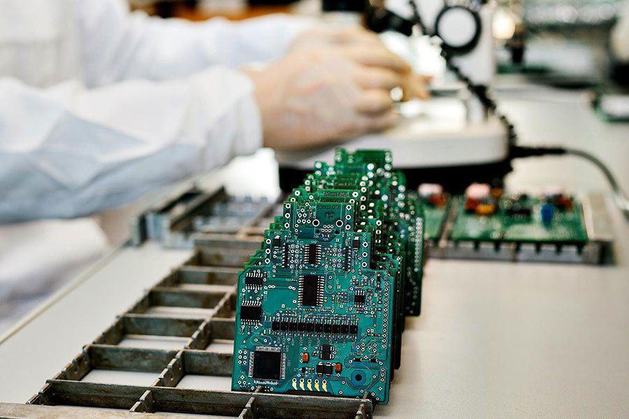
Any-Layer HDI PCB
Any-Layer HDI can be considered a significant step in the evolution of HDI. Any-Layer HDI It is not only hailed for the reduction in the size of the PCB it offers, though it is a significant point in its favor. The superior connectivity and electromechanical properties of the copper filled microvias make Any-Layer PCB very desirable for high-frequency requirements, like that of the 5th Generation telecommunication.
Any layer HDI PCB Design and Fabrication
Any-Layer PCBs can be designed as a core-based PCB, or they can be core-less (IPC Type VI Stackup). Since the Any-Layer HDI doesn’t have any PTH, there isn’t any drilling required after lamination. When you are building with Any-Layer HDI, each HDI layer that is to be stacked on the core’s either side acts as a separate circuit. In each PCB layer, microvias are drilled, then they are filled and plated over, then they are printed over and etched, and finally laminated. If other layers are to be stacked on top, they go through the same process: Drilling, filling, plating, printing, etching, and lamination. If they are working with a plated core, the PCB might have to go through five trips for a 4+2+4 stack up.
But sequential lamination build-up with multiple cycles isn’t the only way. In some cases, a Z-axis conductor paste is applied between all the filled microvias that need to be connected, prior to lamination. And then the layers are laminated together. This reduces the number of lamination cycles required.
Some top-of-the-line fabricators use the Any-Layer Interstitial Via Hole (ALIVH) for Any-Layer HDI PCB fabrication. In it, usually, the microvias are drilled in the prepreg, they are filled with either copper paste or another conductor, which hardens when that HDI layer is laminated. When the layers are ready to be lined up, a unique metallization technique is used to interconnect via holes. This method is a lot superior, both in terms of connectivity, and thermal dissipation, to simply stacking up filled microvias.
Better interconnection of microvias and heat management allows for a higher layer count with Any-Layer HDIs than what might be possible with conventional means.
Special Considerations and Benefits of Any-Layer HDI PCB
Since Any-Layer is a relatively advanced HDI technique, its benefits come with higher costs. The number of lamination cycles alone increases the value of an Any-Layer HDI PCB quite a bit. But there are some other considerations as well.
- 1. The materials should be capable of handling multiple lamination cycles required by an Any-Layer HDI fabrication. Some fabrication materials may be suitable for three repetitions, some six, and some may handle well over ten cycles easily. It is essential to contact your fabricator, go through the guidelines, and the available materials they work with to make sure your Any-Layer HDI is fabricated without time-consuming redesigns.
- 2. Any-Layer HDI allows your fabricator to eliminate the copper plating cycles. These cycles are used in conventional HDI build-ups. This is great for two primary reasons. Firstly, it reduces the overall thickness of the PCB. Second, it improves the electrical and signal carrying capabilities of your PCB by improving the tolerance level of trace impedances.
- 3. it’s a good idea for shielding and ground connections to be edge-plated.
- 4. Any-Layer HDI PCBs reduce the weight of the substrate by almost 60%. Lighter circuits tend to be more jerk and shock-resistant.
- 5. Any-Layer HDI stack up is necessary for Chip Scale Package (CSP) and Inverted Chip Packaging (FC).
DFM for Every Layer Interconnect HDI PCBs
In general, there are a few simple DFM rules that should be followed when floorplanning an HDI PCB that will use ELIC. In addition to following the recommendations of your HDI fabrication house, make sure you implement these general recommendations:
- Choose the appropriate microvia aspect ratio to ensure reliability in the fabricated bare board
- Make sure to specify filled microvias in the internal layers to prevent voiding/dimpling
- Carefully pair up layer thickness with clearance and trace width for impedance controlled lines to ensure you can execute your fanout strategy
- The layer arrangement must be made symmetric throughout the device
Every Layer Interconnect HDI PCB Manufacturing
The ELIC manufacturing process starts with an ultra-thin core with laser-drilled microvias and a solid copper-filled base. After the initial microvia on an inner layer is filled with copper, the next dielectric layer is added in sequential lamination. Laser drilling is applied to the new layer to build the ELIC PCB stacked, followed by filling the vias in that layer with copper. This is repeated until the desired stack is built with copper-filled microvias. The sequential copper fill improves the structural integrity of the board and is needed to prevent dimpling/voiding in the interior microvias as long as buildup produces strong plating interfaces should stacked microvias be used.
Final Words
The most recurrent use of Any-Layer HDIs has been high-end smartphones. But this tech will soon find its way in many other devices as well, especially in products that require high processing power as well as more signal handling capacity.
The best thing about electronics is that it’s always changing. Designers and fabricators are continually pushing the boundaries of what can be done with HDI designs. If you are designing your next circuit using Any-Layer HDI stack up, the first thing you should do is find a fabricator that is capable of realizing your design. Any-Layer HDI requires better lamination capabilities, fabrication facilities, and range of materials, then conventional HDIs.
When you work with us, you will have options beyond industry norms and standards. We can fabricate PCBs with layer counts reaching as high as 68, aspect ratios of 16:1 (much higher than the commonly used ratio of 10:1). Even for blind microvias, we can accommodate aspect ratios of 1.25:1.
For Any-Layer HDIs, we offer copper paste via fills as well as epoxy hole fills. With us, you can build your Any-Layer HDI with 30 layers; this is way beyond what most fabricators can handle. You can even design your HDI in Rigid-Flex if that’s your device’s requirement. Just go through the guidelines, design accordingly, and we will handle the rest.


