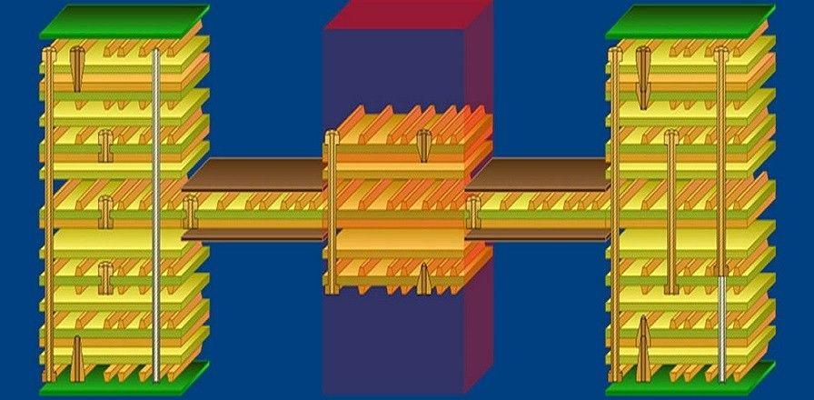
Rigid-Flex PCB Board Stack-up
Rigid-Flex pcb is a vital technology in a world where devices are getting smaller and lighter by the day, without compromising on functionality and reliability. How efficient a Rigid-Flex is in reducing the form factor of conventional PCBs and the overall quality of the circuit depends on how well it’s designed. And a good stack-up is crucial in that regard.
You might be familiar with the layer types in an HDI, where there are proper guidelines and definitions for different kinds of stack-ups. There are no such hard and fast rules for Rigid-Flex stack-ups, but there are some standard and effective design practices. Good stack-ups not only enhance the electrical characteristics of the circuits (no EMI or crosstalk) and mechanical characteristics (proper heat dissipation, flexibility) of a PCB, but they also help reduce the cost of fabricating a Rigid-Flex.
Consequently, if the stack up is poorly designed, the chances of poor Electromagnetic compatibility, stray capacitance, and noise in the circuit get much higher.
Since Rigid-Flex circuits have many more possible applications then a conventional Flex, and it is swiftly replacing Rigid circuits in a lot of applications and designs, cost-controlling is a significant issue. Thankfully, even though fabrication is relatively much more complicated than a Flex or a Rigid PCB, its assembly is more straightforward. And it can be made even simpler with right stack-up strategies.
Rigid-Flex PCB Stack-up
Some of the common considerations in a Rigid-Flex PCB stack-up are:
- An even number of layers is always the most cost-effective. It is usually called asymmetrical construction (or standard construction) of a rigid-flex when the number of layers is even in both the Rigid and the Flex area of the PCB. An example would be a six-layer Rigid-Flex with six layers on the rigid part of the circuit and two on the flex. These designs allow for decent impedance control. Almost three out of every five Rigid-Flex PCBs are made with this stack-up.
- The Flex layer should ideally, always be stacked in the middle of an equal number of rigid layers, in the rigid-flex part of the PCB.
- There shouldn't be any confusion in the stack-up design template of a rigid-flex. This can inconvenience the fabricator and waste a lot of designer's and fabricator's time, both going back and forth on the same design. Make sure to use the software and format recommended by the fabricator while designing your rigid-flex, lest something gets lost in "conversion."
- Properly use the layer stack region feature on your design software to mark the areas which are to act as flex in your Rigid-Flex design. Most people design the rigid-flex as a straightforward board, and defining a uniform stack-up for the complete board, and then marking out the flex region of the board and only leaving the necessary layers on it. This might be easier to do than creating separate stack-up layers for different parts of the board.
- As the number of Flex layers to be stacked increases, try designing with loose leaf construction in mind. No more than two flex-layers per ‘leaf’ is the norm. This allows for higher flexibility and relatively sharper bend radii. But this creates another problem. When you make a bend, the top layer of your flex stack-up bends more than the lowest layer, causing wrinkles and causing fractures in the copper layers, especially around the PTHs. This is especially apparent in radius to thickness ratios less than 6. Its solution is the “book-binder bending” – where you design your flex stack-up in a way that each flex layer is a different length so that when you make the bend, all the layers conform to the same thickness-to-radius ratio. This provides substantial mechanical improvement to the circuit, but it's also relatively pricey due to a higher tooling cost.
- Odd layer stack-ups have some benefits as well. The first thing to understand is that the odd layer stack-up can be independent in the rigid and the flex area of the circuit. You can have an even number of rigid layers and an odd number of flex layers in the stack-up. This is more common than having an odd number of rigid and flex layers in one stack-up.
- The odd number of flex layers (three and above layers) usually allow two-sided shielding of the Flex area. This encourages a stripline impedance control which is desirable in some circuit requirements.
- Some unique impedance requirements (where you need to allot different dielectric thicknesses in different areas of the PCB) might require you to design a Rigid-Flex with asymmetrical stack-ups. It usually drives the cost up. In such constructions, the flex layer isn't right in the middle. Instead, it’s sandwiched between an uneven number of layers of the rigid area of the circuit.
- Another common type of Rigid-Flex PCB stack-up is the integration of ZIF tail in the PCB, on the Flex part. It has two core benefits, saves up space on the rigid section, and eliminates the need for another flex part in the PCB. This reduces space, and it’s also a relatively more reliable stack-up.
- A stack-up type that should be avoided whenever possible is the variable rigid layer stack up. If you want one rigid part of the Rigid-Flex to have eight layers and the other to have four, you will drastically drive the fabrication cost up. First of all, in these types of constructions, most fabricators usually don’t go beyond two different rigid thicknesses. Secondly, it increases the fabrication time, complexity, and cost because the fabrication process has to be duplicated. In the first part of the process, your Rigid-Flex will be fabricated with four layers on all rigid parts of the Rigid-Flex Circuit. Then, the PCB will be rerun through the whole assembly line to stack the additional layers on rigid areas where you want eight layers.
Conclusion
It’s always recommended to go through your fabricator’s guidelines about specific instructions about designing your rigid-flex. This will give you an idea of the scope and limitations of the fabricator, and you can design accordingly.
When you are working with an experienced team, you can explore a lot of options that you might not find with many other fabricators. You can create Rigid-Flex PCBs with up to 20 layers, fine-tune your impedance control, and have a wide variety of materials to work with.


