HDI PCB Stack Up
As the need for high density and highly reliable PCBs increases, High-Density Integration (HDI) PCBs become more and more popular. It's one of the best ways to pack a lot of components and a higher degree of functionality onto a limited board size.
Both designers and fabricators have to improve their conventional methods to match the ever-increasing industry demands of compactness in HDIs. It’s important to understand that some design and manufacturing practices can be both cost-effective and highly result-driven, whereas some wrong practices can adversely impact the HDI PCB production. This is especially seen in HDI stack-ups.
So in this article, we will focus on some of the good and bad practices associated with HDI PCB stack-ups.
The Dos
Some of the good practices that can help you get the best out of your HDI PCB stack-up are:
- Never go beyond your PCB fabricator’s capabilities. Regardless of the layer count, your HDI PCB’s intended application, and the level of compactness you want to achieve, your design should be tailored to stay within your fabricator’s limitations. If you chose the wrong copper weight, smaller or larger drill-hole size, or unbalanced trace widths, you would have to waste a lot of time re-adjusting your stack-up per your fabricator’s specifications.
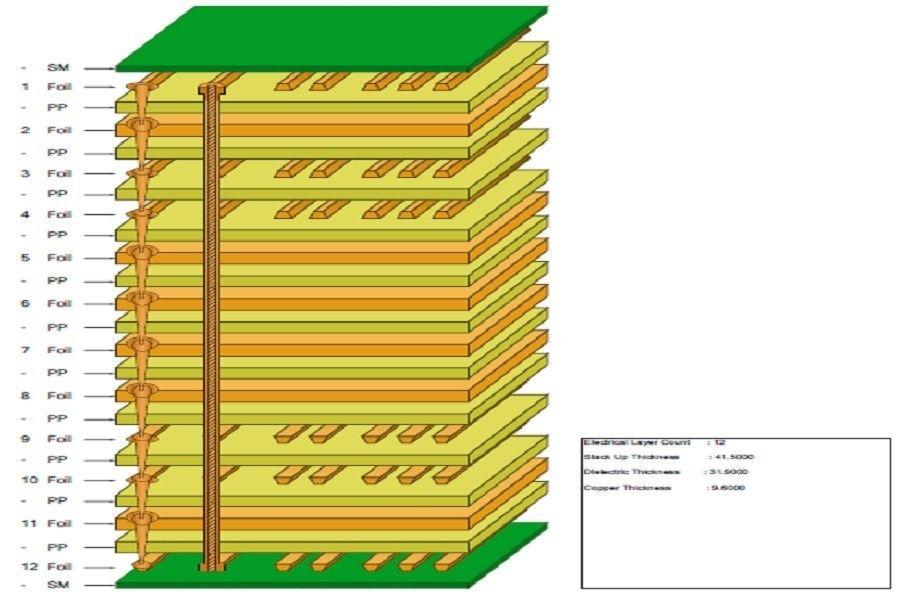
- If you are not sure about the number of stack-up layers your design should have, or how to minimize the number of layers for a particular design, it’s a good idea to involve your fabricator early on in the process. You can consult them for stack-up support. If you are doing it yourself, you have to have the appropriate layer count to accommodate your signal, power, and ground layers. The best practice here is not to get your signal types (high-speed and low-speed) mixed on the inner layers. In a lot of cases, pin density (formula: Area of the board (square inch)/ (Total number of pins on the Board/14)) can help you figure out the accurate layer count. Then you can use a pin density and layer count table to figure out the least number of signal layers you might need.
- The number of layers isn't the only crucial stack-up decision you have to make. Depending on your design and layer count, you should try putting signal and internal power layers. It allows vias between the layers to couple better. Try putting power and ground layers as close together as possible. Route the high-speed layers on the thinnest microstrips.
- Wherever possible, use the same material for all your HDI layers. This prevents the possibility of delaminating, which is mostly an issue with using different materials for different HDI layers because every material has its own moisture absorbance and temperature coefficients. So if the fabrication of HDI with different material layers requires a higher number of temperatures and humidity cycles, the possibility of delaminating gets higher. Tempering to remove it might add to the cost.
- Keeping the power and ground layers adjacent to each other is especially beneficial for the power integrity of the HDI. For configurations where the top two and bottom two layers of the HDI are power-ground couples, the configuration creates distributed coupling capacitances, augmenting the PI of your HDI PCB. The tighter the layers are (with less distance between them), the higher the capacitance you will get. It also increases the resonant frequency of the circuit.
- If both the outer layers of the HDI are ground planes, they can help shield all the internal traces. You can augment that by adding board-level shields and perimeter guard traces in your design. This will result in a fully shielded HDI assembly.
- To reduce the ground impedance, introduce multiple internal (grounded) power layers.
- One of the most important considerations in an HDI stack-up is usually the thickness of signal layers. But if it’s not in conjunction with the thickness of the core, power, and ground layers and prepregs, the resulting thickness of your HDI might off-set your microvia and trace calculations.
The Don’ts
Some of the things you do not want to do with your HDI pcb stack-up are:
- If you have the luxury, never design an HDI that needs more than three sequential laminations. It can drastically increase the fabrication cost. A good way to prevent against designing such a costly stack-up is to plan a good fan-out strategy for your HDI (especially for BGAs and QFNs). A good fan-out plan will help you keep the number of layers to a minimum.
- To prevent any cross-talk in the circuit, try not to put two signal layers adjacent to each other. You can introduce a ground layer in between. This is especially important in high-speed HDIs. A ground plane between to signal layers can also help reduce common-mode interference.
- If cost is your prime consideration, and your layer count is less than eight, don't design an HDI stack-up. But if your design requires a very high layer count (more than eight), then designing in HDI might actually end up cheaper.
- Don’t ignore the importance of process flow in fabrication. If you design holes in the HDI stack-up, without considering the proper conversion and transition between the layers, there will be a lot of issues in the fabrication stage. And it will also drive the cost of your HDI right up.
- Don't go with Type III stack-up if you have a simple enough HDI design that can be realized in Type-I or Type-II. Overcomplicating designing and fabrication will only add to the cost and time to the resulting HDI PCB.
- Don't use stack-up Type IV, V, or VI unless your application specifically requires it. They should only be used for most intricate designs.
Conclusion
Other than the help available on the internet, your best friend in designing the perfect stack-up will be your fabricator. If you consult them early on, they might suggest different, more cost-effective, or efficient stack-ups for your design. Your best HDI pcb design will be realized if you and your fabricator work in relative harmony.


