Step-by-step PCB manufacturing
How is A PCB made Step-by-Step?
Most engineers and designers are mostly concerned with PCB designing and design practices. But that’s like looking at half of the picture and making assumptions based on that. Understanding the steps of PCB manufacturing, its common practices, and especially its limitations can help designers create more manufacturing-friendly designs. This can ensure the cost-effective creation of the final product and limited iterations. The design-for-manufacturing test also gets significantly easier.
Step-by-Step Process of Making a PCB
There are several steps that go into turning a design into the finished circuit that can be installed and used in an electronic device.
Conceptualization and Designing: The first is figuring out your actual circuit needs. This includes the circuit's electrical characteristics, its physical layout, complexity, power needs, etc. If the circuit is made for a device that already has a mechanical design/layout, then the designers have to go around the mechanical constraint and limited space to design the perfect circuit.
The design itself constitutes the bulk of the process. Engineers that understand and follow the design guidelines of their fabricators have adopted some good design practices, usually easing the overall PCB making process. If the design has some fundamental flaws, it's usually destined to go back and forth between the designer and fabricator, until it’s ready to be put into production. Once the design is ready, its’ exported out on a format that the fabricator supports.
DFM and Film: The design goes through DFM checks that are now commonplace with fabricators. These DFM checks save costly time that would have been wasted pulling a PCB midway from manufacturing or assembly. After DFM, the design is printed out on dry-films using a special plotter. Unlike low-cost printers, plotters are capable of printing fine traces and tiny inscriptions.
The final film is different for the outer and inner layers. Inner layers get inked portions for part of the copper that needs to protected and transparent for the part that needs to be etched away. The situation is reversed for the other layers. Registration holes are punched for perfect alignment.
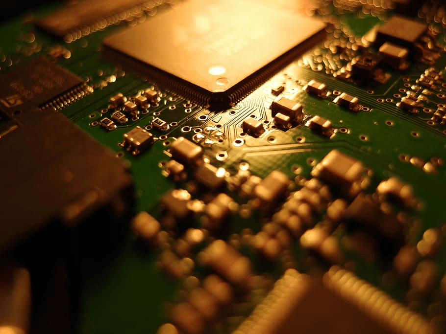
Printing and Etching: Once the film is ready, its time to transfer the pattern over the inner layer. The core in rigid PCBs is usually FR-4, and a copper layer deposited upon it. Since unlike flex, the core doesn't need to constantly bend, fabricators have more options regarding core material and copper. It also gives rigid PCBs more edge when it comes to ground and signal layers. The copper deposited over the laminate core is cleaned because dust or other contaminants can cause shorts in the final circuit and undermine the integrity of the circuit. After that, the photoresist layer, perfectly aligned with the copper-clad core, is exposed to UV light, which hardens the inked pattern on the film, covering the copper underneath.
An alkaline bath removes the film completely, leaving the pattern over the copper. From here on, a simple two-layer board (with just external layers) moves ahead to the drilling sector. For multilayer inner layers printed, the next process is etching. A copper solvent solution dissolves the exposed copper from the layer, leaving the one beneath the ink protected. Now the traces that are beneath the ink need to be exposed. Another solution takes care of that, leaving the relevant copper as the only existing traces on the inner layer.
AOI and Layer Placement: Automated inspection makes sure that there are no issues with the traces. Then the inner layers are aligned with the new layers that need to be pasted on. It’s imperative that inner layer traces are in perfect order because one the inner layers are sandwiched in between, there is no way to fix them. Layers are aligned using the registration holes, and the next layer is placed.
Bonding and Layer-Up: When all the layers are sequentially aligned, they need to fuse together to emerge as the final product. The prepreg needs to be joined with the substrate. Before the press, its imperative that the layers must perfectly align, and there is no mechanical stress, inconsistency, and gaps in the arrangement. Everything needs to fit perfectly because pressing fuses everything together either way. The stack is heated, pressed, and then cooled, all at controlled temperatures. Even an inconsistent cooling can create flaws in the circuit.
Drilling and Plating: An X-ray locator is responsible for finding the right drill holes. For mechanical holes, a buffer material is placed beneath the PCB board to ensure that no unwanted tearing occurs when the via is drilled clean through (for plated-through holes). Many special holes require their own particular drill movement (sometimes angle), so this process takes time. Afterward, a profiling tool shapes the layout of the whole board.
The through-hole needs to plated with thin copper, which is done using a copper deposition. The copper layer is very thin but uniform.
Outer Layer Imaging and Plating: The inverted film is used to transfer the pattern on the outer layer. Cleaned copper is layered over with the film, blasted through UV radiation to harden the copper underneath, then the photoresist is removed. In contrast to the inner layer process, the exposed layer (uncovered part of the photoresist) now needs a copper layer, which happens through the same electroplating process that was responsible for plating the through-holes. The plated copper is covered with Tin to protect it from the upcoming etching stage, which strips away the rest of the copper. After this, the outer (and inner) layer traces are properly established.
Finalizing: Solder mask is applied to protect the copper traces from being oxidized and environmental exposure. Then comes surface finish and silk screening to imprint the important information. After electrical testing to make sure all the traces and vias are functional, the board is ready to be cut into shape.
Final Words
The step-by-step of pcb manufacturing, and by extension, fabricating the final circuit may vary from vendor to vendor. Traditionally, separate manufacturers and assemblers used to increase the time needed to receive the finished product. But nowadays, most seasoned vendors house complete manufacturing and assembly lines under one roof, which is a boon for designers since it cuts down the shipping cost, time, and communication errors between different vendors.


