HDI Printed Circuit Boards or High Density Interconnect PCB: Pros and Cons
With shrinking technology sizes, it's become critical to consider that PCBs with better component density per square centimeter are emerging as a new industrial requirement, particularly in consumer devices; cellphone and PC size reductions are excellent examples. This is where HDI Printed Circuit Boards or High Density Interconnect PCB comes in.
In comparison to traditional circuit boards, HDI PCBs use reduced aspect ratios on the vias, microvias, and laser drilling. They are efficient at supporting electronics with a large number of pins and IC packages with a smaller pitch. Let’s talk about them in detail.
What are HDI Printed Circuit Boards?
HDI or High-Density Interconnect is a PCB with a higher number of interconnections which takes up less space. To classify, an HDI PCB has an average of 120 to 160 pins per every square inch. As an outcome, the circuit board is reduced in size. The elements are closer together, and the board area is reduced dramatically, yet the performance is not affected.
High Density Interconnect PCB technology improves the function of traditional PCBs by optimizing the remaining space and expanding the number of components that can be incorporated into the circuit board. HDI tech opens up space on the PCB by constructing compact components and inserting vias in a more efficient manner. As a result, consumers can benefit from better performance and information storage.
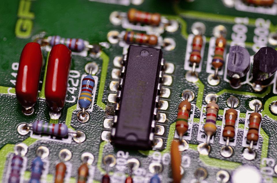
Vias are conductive paths drilled into a multilayered circuit board that act as links in between layers. Vias are a type of vertical trace within a PCB that allow circuit components to be interconnected in these multiple levels. Through-hole vias, buried vias, blind vias, and microvias are commonly used in PCB manufacturing.
Micro vias are commonly seen on HDI printed circuit boards, and they are drilled with lasers rather than regular drill bits. The depth of this form of via is normally limited to two levels. Based on the relative orientation to one another in the PCB, micro vias can be staggered or stacked.
Applications of High Density Interconnect PCB
HDI printed circuit boards incorporate a denser component placement and circuit interconnections. Manufacturers can fit more elements on either side of a raw PCB using HDI technologies.
With the compact size, this technology has allowed manufacturers to design high-performance electronics with a compact size. The examples include mobile phones, laptop computers, touch screens like those found in tablets, and digital cameras, as well as improvements in devices for other industries including medical technology.
Smaller PCBs are very appealing to automobile makers since they conserve space in the vehicle. The incorporation of digital devices to create an improved driving experience has been a primary emphasis of automakers with the advent of revolutionary cars from companies such as Tesla.
HDI is also employed in the armed force industry as well as other strategic weapons such as projectiles and defense systems. As HDI PCBs are very well for harsh environments and dangerous settings, they are a good choice for aerospace and military purposes.
What are the Advantages of Using an HDI PCB?
With HDI printed circuit boards becoming more popular in multiple industries, there is no question that there are numerous advantages of using this type of technology. Some of these are:
- These PCBs use buried vias, blind vias, as well as mircovias, which greatly reduces the requirement of space on the board.
- Their adaptability to applications that prioritize space, performance, and reliability makes them versatile. This allows them to have a similar, or even better, processing power to that of a standard PCB.
- Stacked vias add durability to the design, making them able to withstand extreme weather conditions, which makes HDI PCBs very reliable. As a result, the final design is less vulnerable to faults and far more durable than a standard PCB.
- Via-in-pad, as well as blind via technology, are used in HDI PCBs. This allows the elements to be placed nearer to one another, reducing the distance of the signal path. The HDI technique eliminates stubs, which decreases signal reflections and consequently improves signal quality. As a result of the shorter signal routes, it significantly enhances signal integrity.
- A normal 8-layer through-hole board, which is the requirement for a standard PCB, can be downsized to a 6-layer HDI circuit board without sacrificing the quality.
What are the Disadvantages of Using an HDI PCB?
While the advantages are plenty, there are some drawbacks with manufacturing High Density Interconnect PCB. These are:
- The appropriate materials must be used to build the multilayers. Hence, it requires the use of expensive equipment, which makes it less cost-effective than the standard PCB.
- Vias are utilized in the same way that rivets are used in the assembly process. ROHS puts a lot of heat on the vias. Since the vias are sensitive, they are stressed when the material expands in the z-axis. The current trend is to lower the via diameter while increasing reliability.
- Fiber glass, which is massive for laser drilling, is found in standard pre-pregs. Furthermore, glass in the pre-pregs alters laser direction and results in unsatisfactory or incorrectly shaped laser via holes.
- The plaiting process in the manufacturing of HDI PCBs is also a challenge since it requires you to use the correct aspect ratios while laser drilling.
Final Words
For exquisite precision, HDI PCB manufacture necessitates a high level of technical skill and the most up-to-date state-of-the-art technology.
Hemeixin was one of the first businesses to offer clients high-density connection PCBs in bulk. Our extensive experience and dedication to offering a full solution for our clients’ aids in the resolution of initial design challenges, the reduction of lead time, and the delivery of a high-quality, cost-effective product.
Feel free to contact us and submit your specs for a price if your company is interested in using high density interconnect PCB in its equipment. Our HDI Printed Circuit Board manufacturing experts can analyze your designs and advise you on the right strategy for achieving your objectives.


