What is HDI Stackup
The smaller, the better, right? Or at least that’s what the recent technology trend is. Compacting as much data and functionality into smaller boards or transistors without any physical limits has made it possible for IT companies to create hand-held devices that can perform unlimited functionalities. Here is where HDI PCB comes in. The HDI circuit board optimizes the size of the PCB without affecting the performance and reliability of the device. This is possible due to the cutting-edge HDI PCB stackup technology that enables PCB designers to create multilayer PCBs easily.
In this article, we will discuss HDI PCB stackups and their types. Let’s get started!
● What is HDI PCB?
Before we move on to HDI stackups, we need to know what HDI PCBs are and how they are used.
HDI PCB (high-density interconnector printed circuit board) is a type of PCB with denser wiring per area and is different from conventional circuit boards. The multilayer boards are held together by a lamination process and are electrically interconnected through different vias, depending on the type.
They are smaller in size, have fine lines and wiring, and can enhance the electrical performance of devices.
● Benefits of HDI PCBs
There are multiple benefits of using HDI PCBs, and the major one is the density of the packaging. You can add more components on a smaller board and further reduce the size of the device. Other benefits include:
- HDI circuit boards are smaller and lighter and thus don’t increase the weight of the device.
- They have low power consumption and enhance the electrical performance of the device.
- They increase the speed by faster routing, more component space, and easily placed SMD components.
- Improved signal integrity leads to decreased interference.
- Fewer layers and components can be added on both sides of the layers.
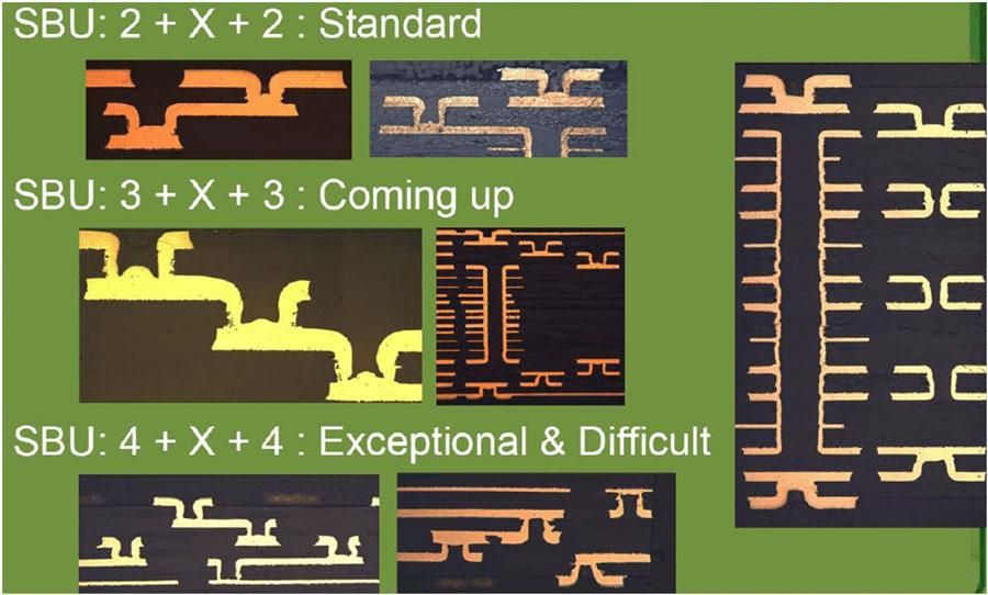
● Types of HDI Stackup
HDI stackup means the number of layers and the process used to create the HDI PCB. It is of three different types, but before we discuss the HDI stackup types, we need to look at the assembly approaches followed by PCB manufacturers.
There are 3 PCB assembly approaches:
- Standard lamination involves the use of through-holes or vias
- Sequential lamination, which involves the use of plated through, blind, and buried vias
- Lamination buildup, which involves the use of micro vias
Each assembly approach has its pros and cons, but the third type is considered most appropriate for HDI PCBs manufacturing. Lamination buildup through microvias is great for devices with fine-pitch and substantial pin-count. Moreover, it provides a larger route density in fewer layers, and its manufacturing is considerably cheaper than the other two assembly methods.
According to the assembly approaches, there are 6 different HDI stackup types (categorized I to VI) available. Out of these 6, only 3 are considered suitable for HDI PCBs. The reasons are higher production costs, complex assembly procedures, and manufacturing challenges. Thus, we will only discuss the HDI stackup I, II, and III.
HDI Stackup Type I
The HDI stackup type I is covered with 1 or more micro vias on both sides but can be placed on a single side as well. It utilizes buried vias and plated through vias, but buried vias cannot be used.
The number of layers in stackup type I is dependent on 2 factors: the FR-4 dielectrics and the ratio factor.
● If you are using FR-4 dielectrics with very thin characteristics, they can easily delaminate under extremely high temperatures, which may be applied to perform a lead-free method of smoldering.
● For ensuring reliability and enhanced electrical performance, the ratio factor of length to the hole diameter in the PTH via needs to be kept smaller than 10.
The HDI stackup type I is not suitable for high-dense boards. You would need to increase the dimension to add more layers because a microvia on a single layer does not provide sufficient performance advantages.
HDI Stackup Type II
In HDI stackup type II, you can utilize buried, blind, and micro vias on a laminated core. It is also necessary to add micro vias on 1 or more sides; both sides are unnecessary.
Manufacturers can use different assembly approaches to build HDI stackup type II. Depending on the micro via, they go for whether stacking on staggering.
The HDI stackup type II is preferred and suitable for high-density boards because they are more stable, handle extra layers and components, and enhance functionality in the same dimension. Although, there are some constraints, like with HDI stackup type I, you can only place the micro vias on the outer layers, which is unsuitable for some projects.
HDI Stackup Type III
In this HDI stackup type, you can utilize blind, buried, and micro vias over a laminated core. The only major difference between type II and type III HDI stackup is that you put 2 or more micro via layers on the side, and you do not have to put them on both sides.
The HDI stackup type III is also suitable for high-density boards with multiple layers and big BGAs with fine-pitch features. The constraints faced with stackup types I and II are also eliminated as the manufacturers can place the micro vias in the inner layers and use them for power planes and grounds.
The extra number of layers means a better routing signal and increased speed. The manufacturing process is expensive compared to the other two types, but the investment is worth it.
● HDI PCB Design Considerations
Depending on the complexity and need of the project, the HDI PCB design guidelines can vary. We need to factor in the physical, thermal, and electromagnetic constraints to avoid problems in the design process. There is electronic design automation software available nowadays to remove design complexities. Before these, manufacturers had to analyze the following factors:
1. Electromagnetic interference: optimizes the high-speed signal design and removes constraints like noises and accidental antennas.
2. Thermal: as mentioned above, micro vias can cause delamination under high temperatures, thus keep thermal performance under check.
3. Impedance control: to maintain good signal integrity, you need to keep the ratio factor under 10 and the dielectric thickness, traces, and spacing.
Now that you know all about HDI PCBs and their stackup types, you can choose the right type for your project. Instead of designing one yourself, it’s best to consult PCB manufacturers for assembling or choosing the right fit for your project.


